Modeling of High-Speed PCB-Interconnects, Vias and Connectors for the Estimation of SI-Losses
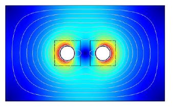
Estimation of both single-ended (SE) and differential-pair (DP) impedances of high-speed PCB-traces/interconnects, vias and connectors is very important for the high-speed PCB (layout) design. This is because, the mismatch in line-impedances/improper line-termination results in a significant loss or distortion of high-speed digital signals at the receiver side. This happens mostly due to signal reflection/crosstalk between neigboring parallel lines during transmission of high-speed digital signals through PCB-interconnects/vias and connectors etc. In order to estimate the amount of reflected signal/SWR or signal-integrity (SI) losses, and also the SE/DP-impedances, initially 2D geometry models of vias/connector (as depicted in Figures-1 and 2) were developed and frequency domain simulation with a frequency sweep from 1.0 GHz to 10 GHz were carried out with ec and mf-physics interfaces of Comsol Multiphysics ® to extract the RLC-parasitic elements of the vias/connector at different operating frequencies. Figure-3 shows the frequency domain simulation of high-speed vias/signal connector for the estimation of single-ended impedance of the latter. Similarly, Figure-4 shows the frequency domain simulation of high-speed vias/signal connector for the estimation of differential-pair impedance of the connectors as depicted in Figure-1 (2D model) and Figure-2 (3D model). As the reflection co-efficients are function of SE/DP-impedances and the latters are the function of RLC-parameters at the operating signal frequency- the reflection co-efficients were estimated using the following formulae: Z0 = sqrt of (L/C) and Reflection = (Z0-ZL)/(Z0+ZL). Further simulations were carried out developing a 3D-geometry model of the connectors using Comsol Multiphysics® and results will be reported later in the full paper.
Download
- palit_presentation.pdf - 0.68MB
- palit_abstract.pdf - 0.09MB