Reflow soldering in IC packaging
Application ID: 120151
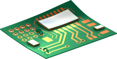
Reflow soldering is an important process in IC packaging. In reflow soldering, the solder materials are melted to create joints between electrical components and the PCBs for structural and electrical connections.
This model demonstrates the process of attaching chips to a PCB by reflow soldering. The model is implemented using the “Activation” feature. Due to different thermal expansion coefficients of the materials, residual stresses remain in the final product. This leads to warpage of the PCB and stress concentration in the solder joints.
In this model, the temperature change is described by a user-defined function. For further extension, the heat transfer between the structure and the surroundings can be considered to obtain detailed temperature distribution and evolution. In addition, more complex constitutive models such as viscoplasticity models can be applied for the behavior of solder materials at high temperature.
This model example illustrates applications of this type that would nominally be built using the following products:
however, additional products may be required to completely define and model it. Furthermore, this example may also be defined and modeled using components from the following product combinations:
The combination of COMSOL® products required to model your application depends on several factors and may include boundary conditions, material properties, physics interfaces, and part libraries. Particular functionality may be common to several products. To determine the right combination of products for your modeling needs, review the Specification Chart and make use of a free evaluation license. The COMSOL Sales and Support teams are available for answering any questions you may have regarding this.