The Application Gallery features COMSOL Multiphysics® tutorial and demo app files pertinent to the electrical, structural, acoustics, fluid, heat, and chemical disciplines. You can use these examples as a starting point for your own simulation work by downloading the tutorial model or demo app file and its accompanying instructions.
Search for tutorials and apps relevant to your area of expertise via the Quick Search feature. Note that many of the examples featured here can also be accessed via the Application Libraries that are built into the COMSOL Multiphysics® software and available from the File menu.

This model and tutorial demonstrates the use of an Application Method to compute and plot the geometric Modulation Transfer Function (MTF) for the Petzval Lens. Read More

This model demonstrates how to simulate surface plasmon polaritons in a thin metal layer embedded in dielectric layers. It calculates the dispersion and propagation length of surface plasmon polaritons as a function of photon energy. Read More

This tutorial shows how to set up a multi-element objective lens. The chosen lens is the Double Gauss described in 'Modern Lens Design (2nd edition)', by W. Smith, 2005, pg 323. The tutorial demonstrates how to create a geometry sequence using the 'Spherical Lens 3D' part found in the ... Read More
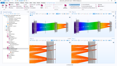
This tutorial shows how to set up a multi-element objective lens. The chosen lens is a Petzval lens with field flattener described in 'Fundamental Optical Design', by M. Kidger, 2001, pg 192. The tutorial demonstrates how to include a geometric sequence using the 'Spherical General Lens ... Read More

This example demonstrates how to optimize the thickness of a microelectromechanical systems (MEMS) mirror coating material for maximum reflectivity. To reduce the simulation time, a Layered Impedance Boundary Condition is used to model the thin coating material on top of the metallic ... Read More
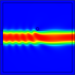
This model includes a dielectric slab waveguide with a small lossy metallic object nearby. The object causes light to be scattered, absorbed, and both reflected and transmitted along the waveguide. Learn more in this accompanying blog post: Modeling a Scatterer Near an Optical Waveguide Read More

Microlithography lenses are used to project the image of an integrated circuit onto a silicon substrate. This tutorial demonstrates how to create a 21-element fused silica lens which has a NA of 0.56 which is designed to be used at a wavelength of 248nm. The lens, which has a total ... Read More
This example shows how to perform parameter optimization on a lens system. The optimization is motivated by the replacement of one of the glasses in a prior optical prescription with a new glass having slightly different optical dispersion coefficients. The control parameters are the ... Read More

In its simplest form, an optical ring resonator consists of a straight waveguide and a ring waveguide. The waveguides are placed close to each other, making the light affect each between the two structures. If the propagation length around the ring is an integral number of wavelengths, ... Read More

This model demonstrates how to use topology optimization with milling constraints to design a metalens that focuses a single wavelength to a point. This involves transferring the optimized results to another component so the result can be verified using an explicit geometry ... Read More