FEM modeling of highly strained monocrystalline ZnTe/CdTe core-shell hetero-nanowires
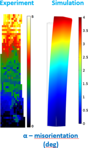
The monocrystalline semiconductor nanowires (NWs) attract great interest as they reveal new properties that differs from the ones of the bulk equivalents. In addition to small size (10-100 nm diameter), one of their advantages is extremely high surface to volume ratio. This determines the widespread use of NWs for various sensing, nanoscale optoelectronics and photonics applications. Hetero-NWs are required in most cases to reveal the full potential of NWs based devices. NWs consist from two or more crystals in axial or radial (core-shell) configuration. Coherent or semicoherent (partially relaxed) structure can be obtained even for a high lattice mismatch systems as (Cd, Zn)Te where the relaxed lattice parameters of compounds differ by 6.2%. The monocrystalline core as well as epitaxial shells can be grown by Molecular Beam Epitaxy (MBE) in one process. The significant strain fields can cause surface morphological transformations of the NW to minimize free energy. Moreover, the core-shell NWs are very sensitive to radial inhomogeneity. Even slight asymmetry of concentration or core decentering leads to occurrence noticeable strain/asymmetric force distribution, and as result the bending of NWs. Implementation the core-shell configuration will introduce to complex anisotropic 3D lattice distortion comparing to 2D tetragonal distortion of epilayers on thick substrate. The strain distribution has a big impact on the optical and electronic properties of NWs. Therefore, understanding the mechanism of the relaxation process is crucial for the further application of NWs. Transmission Electron Microscopy (TEM) is one of the well designated and versatile tool for structural investigation of nano- and micro-objects with sub-nanometer resolution. The Scanning Nanobeam Electron Diffraction (NBED) technique was used to obtain 2D residual strain map for individual nanowires. The 2D maps of residual strain components in axial and radial directions were obtained using new developed software for analysis of the series of NBED patterns. Moreover, local orientation maps for bended NWs were obtained using analysis of diffraction intensity distribution by pattern matching technique. Finally, Finite Element Method (FEM) simulations were used for a comprehensive study of strain distribution and morphological transformations of hetero-nanowires. The obtained results agrees qualitatively with the experiment. However the crystal anisotropy, nonlinear behavior of material under extreme stress of tens of GPa as well as the surface tension, piezoelectric and magnetostriction properties of low symmetry nanocrystals, need to be taken into account in future model. We present experimental data and initial anisotropic FEM model of elastic relaxation of core-shell nanowires, to discuss the possibilities of improving our initial model with more advanced Comsol users. We believe that our experimental data will contribute to improvement and validation of the calculation methodology suitable for even more complex Nano devices based on magneto-piezoelectric NWs. This research is supported by UMO-2016/21/B/ST5/03411
Download
- COMSOL 2020 final.pptx - 5.95MB