Studying the plasmonic properties of smooth, rough and nanostructured gold surfaces
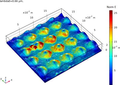
In order to better understand the effect of controlled surface topographical features on SERS (surface-enhanced Raman scattering) enhancement factors, simulations of plasmonic properties of different gold surfaces (smooth, rough and nanostructured) have been carried out using the finite-element method (COMSOL Multiphysics®) and a paraxial Gaussian beam approach (included in the Wave Optics Module). The smooth surface has been simulated with COMSOL Multiphysics® and the rough and nanostructured surfaces were imported from atomic force microscopy (AFM) data. Gold thin film were deposited using a conventional thermal evaporation on both a silicon wafer to form a 100 nm thick film with an average surface roughness of 2 nm and on our patented nanostructured support (height= 110±10 nm, width= 450±5 nm). The experimental AFM surfaces were imported using a linear interpolation and parametric surface (Fig. 1). Our model was set up with only two domains (Fig.2); the gold film was modelled using the LorentzDrude dispersion model and the above medium was defined as air. The Wave Optics module which includes “Electromagnetic Waves, Frequency domain interface” allows us to use a paraxial Gaussian beam (top boundary), Eb (x,y,z)= Ebg0 w0/(w(z)) exp[-p^2/(w^2 (z) )-jkz-jk p^2/2R(z) +jn(z)], with waist w0, focal p0 and k vector. Due to the polarization selectivity of the plasmon excitation, the incident source was polarized with the electric field parallel to the surface and the calculation were made over the 360 °. The simulations cover wavelengths of 400-800 nm in order to identify plasmonic resonances and their dependence on geometry parameters (Figure 3). As expected, the maximum intensity of the localized EM field is lower for a smooth surface than a rough surface and increases for a nanostructured surface. Figure 4a shows the local EM field distribution for the nanostructured surface with an enhancement of the EM field (“hotspot”) mainly on the top of structures. The average of the EM field norm on the different surfaces was calculated, which allows to study the evolution of these values as a function of the incident wavelength (Figure 3). In order to investigate experimentally the SERS performances of our rough and nanostructured supports, SERS imaging were performed at 660 nm after immersion of the substrates in a 10−6 M solution of thiophenol (Figure 4b). The Raman intensity is higher on the nanostructured surface than the rough gold film (Figure 4c), and the enhancement factors are in good agreement with our calculations, thus confirming the validity of our simulation approach. Convinced by these preliminary results, we will therefore exploit these new possibilities offered by COMSOL Multiphysics® to further direct the design and the elaboration of more complex nanostructured surfaces and predict the plasmonic properties of our engineered surfaces.