ECAD Import Module

Import ECAD Files into COMSOL Multiphysics®

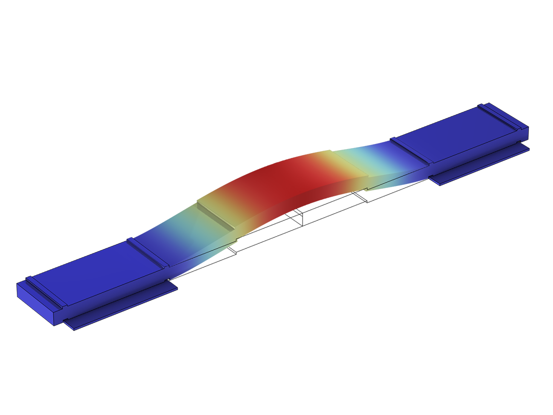
The ECAD Import Module extends the capabilities of COMSOL Multiphysics® with functionality for importing popular layout formats for microelectromechanical systems (MEMS) devices, integrated circuits (ICs or chips), and printed circuit boards (PCBs). Layouts in the GDS-II, IPC-2581, and ODB++ formats can be imported and automatically converted to 3D geometry models suitable for analysis. The module also includes export functionality for sharing designs in the OASIS format, an industry standard for photomask exchange. The ECAD Import Module can be combined with other modules in the COMSOL product suite to simulate a variety of application areas, including low- and high-frequency electromagnetics, heat transfer, structural mechanics, and microfluidics.

Contact COMSOL
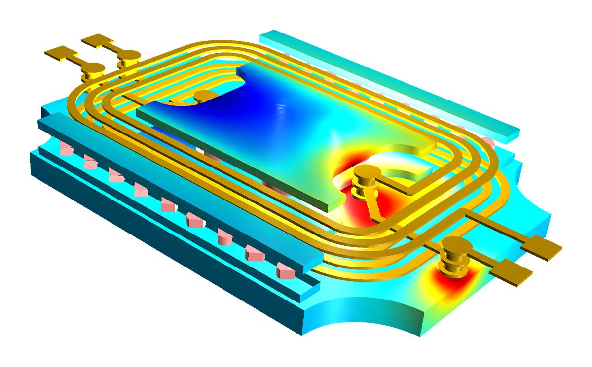
A PCB model showing the electric field norm in the dB scale.

Treating Imported ECAD Files

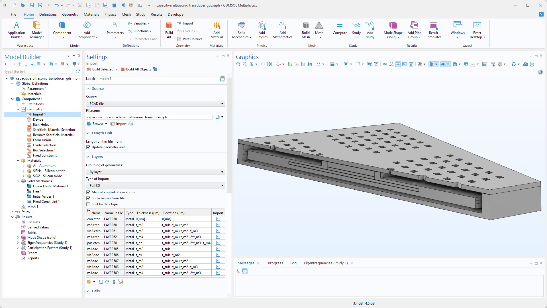
Depending on the file format, the import functionality provides different options for configuring how the geometric shapes contained in the layers of imported ECAD files should be used for geometry construction. Layers can be selected for import, layer thicknesses and elevations can be edited, and parameters can be fine-tuned to simplify the geometry. For a faster setup of the import process, the layer configuration information can be loaded from a text file. To further shorten the time spent on setting up simulations, the import can be configured to automatically create selections for each layer. These selections are then available when assigning physics settings to domains and boundaries.

The 3D geometry objects constructed from the ECAD layouts are represented in the software just like any other 3D model and can be further edited using the geometry modeling features in COMSOL Multiphysics®.

When the ECAD Import Module is combined with the CAD Import Module, the Design Module, or one of the LiveLink™ products, 3D geometry can be exported to the IGES, STEP, ACIS®, or Parasolid® file formats for use in other software.
PCB Layouts

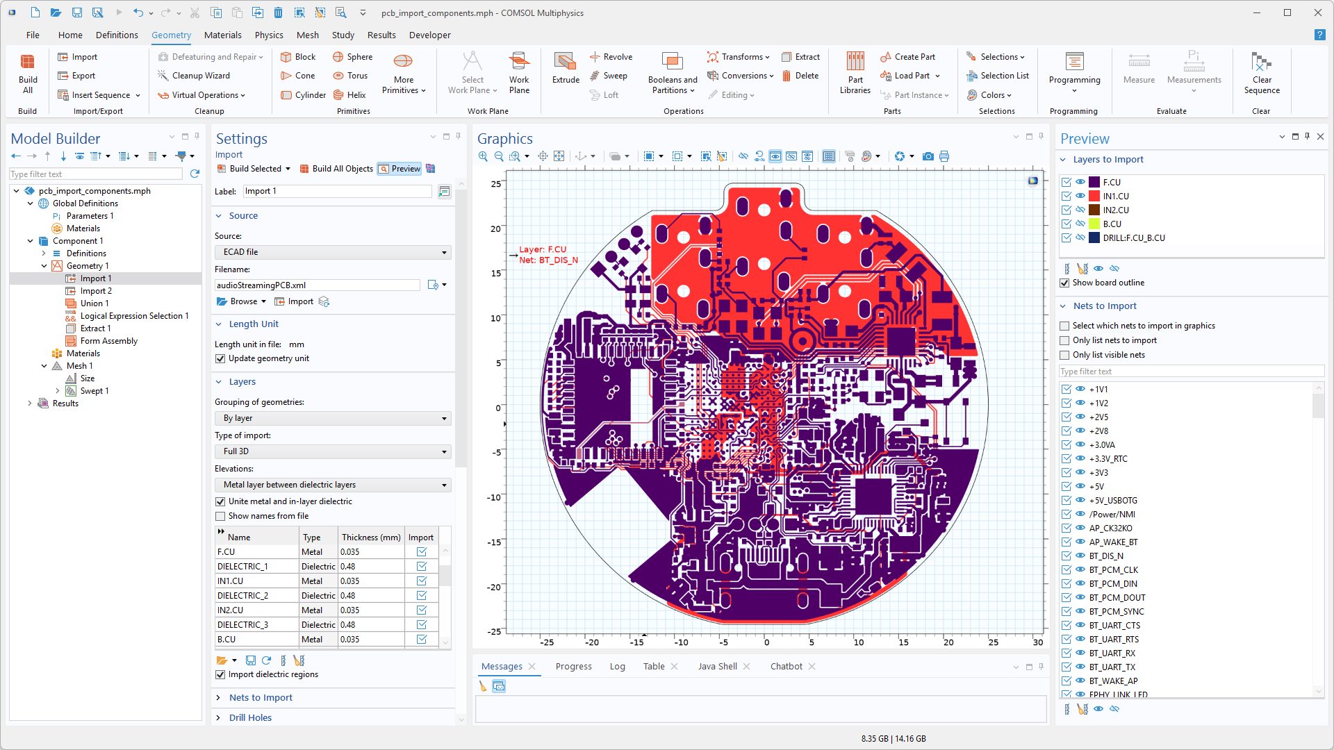
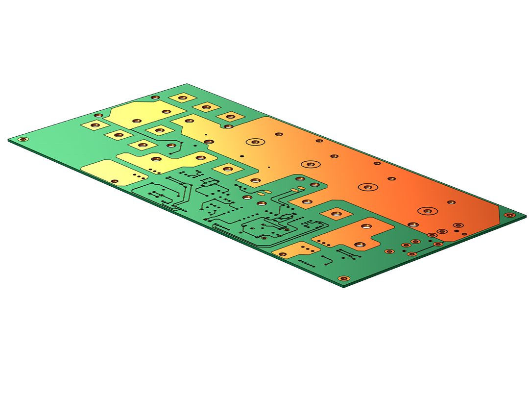
The IPC-2581 and OBD++ file formats can handle most of the information needed to manufacture a PCB, including copper and dielectric layers as well as component footprints and outlines. Before import, the PCB layer layouts can be previewed, and the information to include can be selected.

For generating a geometry for simulation, the import functionality can read some of this information, including the layout of the copper, dielectric, and via layers; the board outline; component outlines; and the layer stack-up information. An ECAD file for PCBs may also include information about the electrical nets that the copper traces and vias are part of. Users can choose to import either all or a selection of the available nets and then configure the import to use this information to generate selections. Domains created for pads and components can be identified using attributes such as component names, pin numbers, and electrical nets. The selections and attributes generated during import are useful when preparing the geometry for simulation and when setting up the physics and mesh.

Creating 3D Models for Circuit Boards

To obtain a 3D geometry, the PCB importer first generates the 2D geometry representing each layer by combining the shapes defined in the layout mask from the file. To avoid the very short edges that are often present when generating the geometry for copper traces, the import can be configured to eliminate short edges and ignore vertices with continuous tangents.

Users can choose to keep the copper layers as surfaces in the geometry, which can be useful when approximating the traces as shells, or the layers can be extruded automatically according to the layer stack-up. This information can be read from the IPC-2581 and OBD++ file, and users can also enter it directly or import it from a separate text file.

Via layers can be extruded and included in the 3D geometry for the PCB with options to create domains for the via plating and via core, making it possible to model both open and plugged vias.

When combined with the [Design Module][/design-module], the ECAD Import Module enables further modification of the 3D geometry of a board, such as adding fillets to corners, as well as integration of the PCB geometry with imported CAD designs, for example, the device that contains the PCB. The 3D geometry of an imported PCB can also be exported to CAD formats for use in other programs.

IC and MEMS Layouts

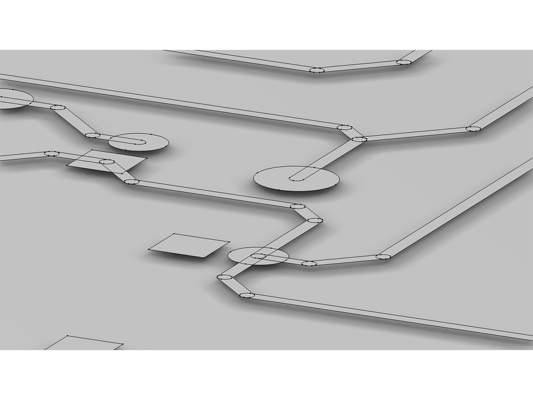
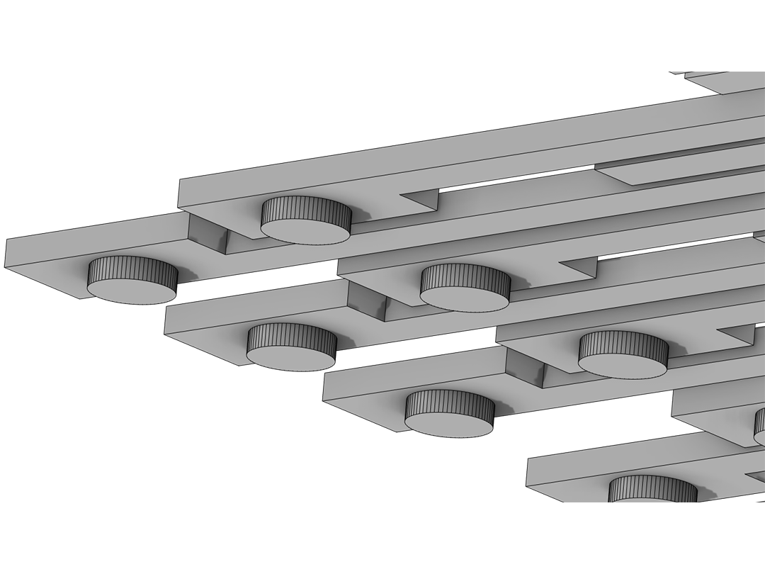
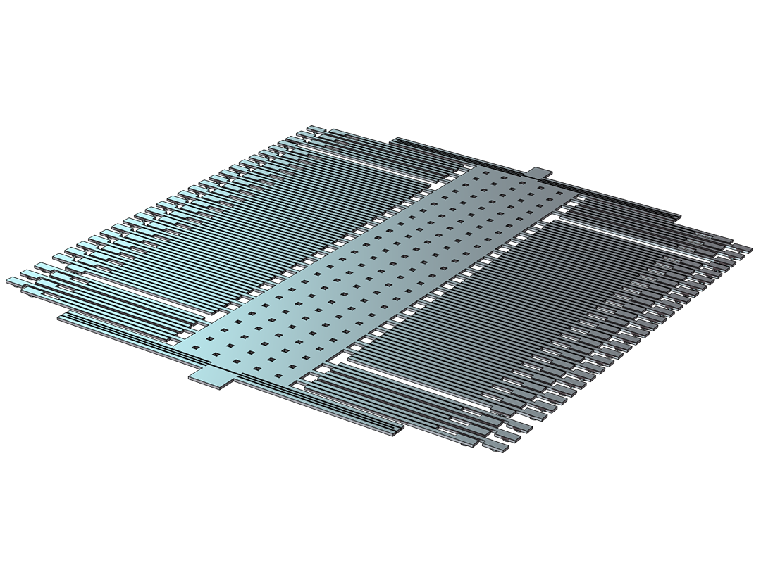
The GDS file format (GDS-II) is commonly used when transferring the layer masks for the fabrication process of ICs and MEMS devices. The file is binary, with the shapes on the layers made of polygons — these can be organized into libraries called cells, which can be instantiated into other cells and layers. The different layers usually represent different steps in the manufacturing process, and the import can be configured to generate the geometry for selected cells and layers. The import can also recognize the data type that is sometimes used in GDS files to further differentiate between the polygon shapes on the layers.

For an efficient workflow, users can select the option to automatically assign the geometric entities and objects generated by the GDS importer to named selections based on the layers, cells, and data types that the imported shapes belong to.

These selections are then available as input in downstream geometry operations and when setting up the physics and the mesh.

Creating 3D Geometry from GDS Files

To generate geometry objects suitable for simulation, the GDS importer automatically recognizes arcs and straight lines, and thereby eliminates the short edge segments that would otherwise result in an unnecessarily fine mesh. In addition to the arc and line recognition, the same options for removing short edges from the resulting geometry can be used for importing layouts for PCBs.

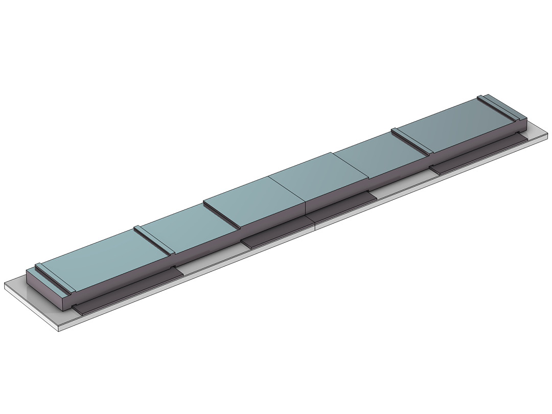
The GDS format does not specify how the layers should be used for the fabrication process; this information is usually supplied in some other way. When importing a GDS file, a thickness and elevation for each layer can be configured to create a 3D structure by extrusion. This method is suitable when a layer is deposited and patterned over a flat surface and contains the mask for a positive photoresist.

Modeling Devices with Complex 3D Structures

To create more complex 3D structures, the geometry objects generated by the GDS import can be combined with other geometry objects via Boolean geometry operations. For example, when importing the mask for a negative photoresist, the extruded layer can be removed from other objects after the import by using a Boolean difference operation.

When the ECAD Import Module is combined with the Design Module, users can also efficiently emulate semiconductor fabrication processes where the layers are deposited and patterned over nonflat surfaces. This is done on the geometry by offsetting, in the normal direction, the faces where the layer is to be deposited. The resulting object is then intersected with the extruded layer mask from the GDS file to create the geometry for the patterned layer.

Parasolid is a registered trademarks of Siemens Product Lifecycle Management Software Inc. or its subsidiaries in the United States and in other countries. ACIS is a registered trademark of Spatial Corporation.

Support for implementation of the ODB++ Format was provided by Mentor Graphics Corporation pursuant to the ODB++ Solutions Development Partnership General Terms and Conditions.

Every business and every simulation need is different.

In order to fully evaluate whether or not the COMSOL Multiphysics® software will meet your requirements, you need to contact us. By talking to one of our sales representatives, you will get personalized recommendations and fully documented examples to help you get the most out of your evaluation and guide you to choose the best license option to suit your needs.

Just click on the "Contact COMSOL" button, fill in your contact details and any specific comments or questions, and submit. You will receive a response from a sales representative within one business day.

Next Step

Request a Software Demonstration