Electron Beam Crystallization of Amorphous Silicon Thin Films
Published in 2016
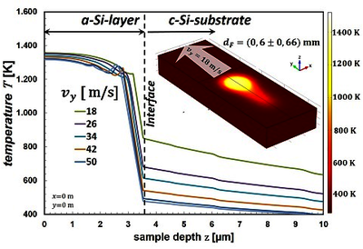
A promising method for low cost production of efficient silicon thin film solar cells is the electron beam physical vapor deposition (EB-PVD) of high purity amorphous silicon (a-Si) layers with high deposition rates up to 300 nm/s [1] followed by crystallization. This study focuses on EB crystallization of deposited a-Si films in the solid phase regime and justifies observed experimental results by simulations. The simulations were carried out to clarify delamination phenomena. Therefore, a structural and thermal investigation of the pre-stressed substrate-layer-system was carried out using different speeds of the EB for a given line pattern and absorbed EB power-depth-relation.
Download
- saager_presentation.pdf - 2.06MB
- saager_paper.pdf - 0.96MB
- saager_abstract.pdf - 0.75MB