Besi Improved Memory Chip Manufacturing with Multiphysics Simulation
Stefan Behler, Besi, Switzerland
As memory chips become smaller and smaller, designers must ensure that the chips stay intact during the manufacturing process. Besi develops equipment and assembly processes for substrate and wafer packaging production in markets such as consumer electronics, automotive, industrial, and solar energy. Stefan Behler, a senior expert process engineer, used multiphysics simulation to explore and optimize a new way of peeling off the tape on a memory chip that results in less deformation of the dies. This new method is now used by semiconductor packaging factories all over the world.
Suggested Stories
The Sight of Sound: Revealing the Effects of Enclosure Design on Loudspeaker Performance
L-Acoustics uses acoustics simulation to optimize their bass reflex speakers for sound systems in arenas and concert ...

Designing the Sound Absorption of Microlattice Structures
Using numerical simulation, you can design microlattice structures with sound-absorbing properties, and then print ...
Precision Performance: The Pursuit of Perfect Measurement
Brüel & Kjær, a manufacturer of transducers, microphones, and other instruments and software for sound and ...
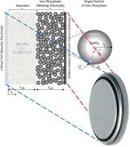
Highly Accurate Li-ion Battery Simulation
Battery management systems (BMSs) are designed to protect the batteries and predict their charge level. They use ...