
Besi Improved Memory Chip Manufacturing with Multiphysics Simulation
Stefan Behler, Besi, Switzerland
As memory chips become smaller and smaller, designers must ensure that the chips stay intact during the manufacturing process. Besi develops equipment and assembly processes for substrate and wafer packaging production in markets such as consumer electronics, automotive, industrial, and solar energy. Stefan Behler, a senior expert process engineer, used multiphysics simulation to explore and optimize a new way of peeling off the tape on a memory chip that results in less deformation of the dies. This new method is now used by semiconductor packaging factories all over the world.
Suggested Stories
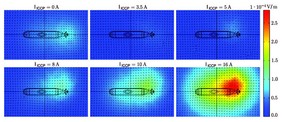
Submarines: Corrosion Protection or Enemy Detection?
Submarines create underwater electric potential (UEP) signatures when using corrosion protection systems. These ...
Illuminating Complex Material Behavior with Multiphysics Simulation
At Canadian Nuclear Laboratories, multiphysics simulation is used to gain insight into the behavior of nuclear fuel ...
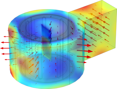
Developing a New Microreactor for Organic Synthesis Using Microwave Heating
The chemical reactions used to generate solvents and certain pharmaceuticals rely on organic synthesis, a process of ...
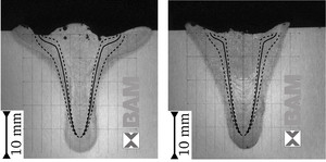
Magnets Improve Quality of High-Power Laser Beam Welding
High-power laser beam welding uses a localized heat source to achieve narrow deep welds and high welding rates. ...


