
Besi Improved Memory Chip Manufacturing with Multiphysics Simulation
Stefan Behler, Besi, Switzerland
As memory chips become smaller and smaller, designers must ensure that the chips stay intact during the manufacturing process. Besi develops equipment and assembly processes for substrate and wafer packaging production in markets such as consumer electronics, automotive, industrial, and solar energy. Stefan Behler, a senior expert process engineer, used multiphysics simulation to explore and optimize a new way of peeling off the tape on a memory chip that results in less deformation of the dies. This new method is now used by semiconductor packaging factories all over the world.
Suggested Stories
Identifying the Root Cause of Electronics Failures with Simulation Apps
The Centre for Electronic Corrosion (CELCORR) research group at the Technical University of Denmark predicts ...
Optimizing the Performance of Complex Building Façades
Engineers at Newtecnic specialize in complex building design, working with bold and fluid architectural shapes. To ...
Multiphase Flow Simulation Guides Wastewater Treatment Plant Design
To improve the health of the Dommel river, an aeration unit has been added to the Eindhoven wastewater treatment plant ...
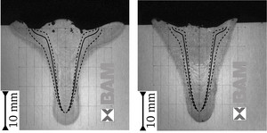
Magnets Improve Quality of High-Power Laser Beam Welding
High-power laser beam welding uses a localized heat source to achieve narrow deep welds and high welding rates. ...


