
Besi Improved Memory Chip Manufacturing with Multiphysics Simulation
Stefan Behler, Besi, Switzerland
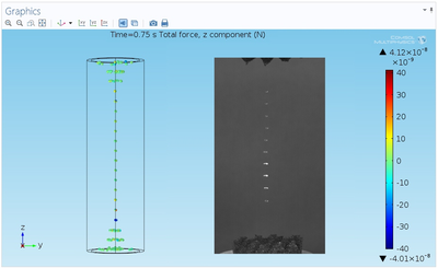
As memory chips become smaller and smaller, designers must ensure that the chips stay intact during the manufacturing process. Besi develops equipment and assembly processes for substrate and wafer packaging production in markets such as consumer electronics, automotive, industrial, and solar energy. Stefan Behler, a senior expert process engineer, used multiphysics simulation to explore and optimize a new way of peeling off the tape on a memory chip that results in less deformation of the dies. This new method is now used by semiconductor packaging factories all over the world.
Suggested Stories
Lighting the Way for Improved Synchrotron Vacuum Chambers at RadiaSoft
One of the goals of the Argonne National Laboratory (ANL) is to increase the brightness of synchrotron beams for the ...
Greening the Heart of the City: An Urban Rooftop Drainage System Inside a Garden Fence
TL-Engineering, a simulation consultant, teamed up with a professor, civil engineer, and sound barrier company to ...
Designing a Miniaturized Wastewater Treatment Plant for Micropollutant Degradation
Eden Tech uses multiphysics simulation to design a miniaturized wastewater treatment system made from compact discs. ...
Floating on Sound Waves with Acoustic Levitation
As part of an industry that saves lives on a regular basis, pharmaceutical companies are in need of systems that can ...


