
Besi Improved Memory Chip Manufacturing with Multiphysics Simulation
Stefan Behler, Besi, Switzerland
As memory chips become smaller and smaller, designers must ensure that the chips stay intact during the manufacturing process. Besi develops equipment and assembly processes for substrate and wafer packaging production in markets such as consumer electronics, automotive, industrial, and solar energy. Stefan Behler, a senior expert process engineer, used multiphysics simulation to explore and optimize a new way of peeling off the tape on a memory chip that results in less deformation of the dies. This new method is now used by semiconductor packaging factories all over the world.
Suggested Stories
Enhancing Performance and Safety of Medical Implantable Devices with Multiphysics Simulation
At Abbott, Freddy Hansen uses multiphysics simulation to model left ventricular assist devices (LVADs) to improve the ...
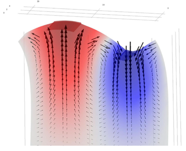
Gaining Insight into Piezoelectric Materials for Acoustic Streaming
Many sensors, such as flow sensors and those used in medical diagnostics, rely on microfluidic devices. However, ...
WiTricity Leverages Magnetic Resonance for Flexible Wireless Charging
Engineers at WiTricity have developed a flexible wireless charging setup that relies on magnetic resonance and can be ...
Increasing Productivity and Revenue with Computational Applications
HeatSinkSim is a simulation app created by the specialists at AltaSim Technologies that can help optimize heat sink ...


