COMSOL® Modeling of Self-Limiting Electrospray Deposition
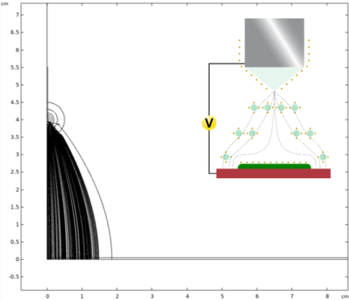
Electrospray Deposition (ESD) is a process used in manufacturing that utilizes a charged capillary to disperse a flowing liquid into a spray that deposits onto a grounded target substrate. The build-up of charge on the substrate can begin to deflect further spray, allowing the material to spread out over the surface over time, resulting in self-limiting electrospray deposition (SLED). The SLED process can be extremely advantageous in manufacturing coatings as the spray will be attracted to grounded targets, allowing spray to not be wasted. To understand how SLED coatings evolve over time, COMSOL® can be coupled with MATLAB® scripting to model the electrospray process and determine the thickness and charge over a sprayed surface. This COMSOL® set-up utilized a 2D-axissymmetric model, the AC/DC Module, and electrostatics interface. A rectangle geometry with a set electric potential was used to model the needle, and another rectangle geometry was used with a zero charge boundary to represent the area surrounding the spray with the bottom side set as a ground to represent the grounded substrate. A structured mesh was used. A line above the ground was used with a surface charge density to represent the charge build-up over time. This surface charge density was defined as a MATLAB function that computed the charge build-up. A particle trace located below the needle was used to find the final locations on the substrate of the sprayed particles. Using this particle trace, the MATLAB function defining the surface charge density would compute the new surface charge on the film, which would allow the SLED properties of the spray to be displayed. This model was run iteratively using a MATLAB wrapper to model the ESD of the film over time. This was done on different axisymmetric substrate geometries such as a flat, cylinder, or needle geometry. Alternate surface charge density MATLAB functions were also used to model a substrate with alternating conductive and nonconductive strips. Using COMSOL’s modeling software to find the films of different ESD substrates can allow us to understand film growth for different manufacturing purposes, especially using SLED to coat 3D surfaces. It can also help us quantify the amount of spray lost to nonconductive surrounding surfaces, as a main advantage of SLED is how little spray is wasted in manufacturing.