Equation Based Modeling of MOSFET
Introduction
In this work, we will present an equation based technique for MOSFET simulation in COMSOL 5.4 and will discuss about the challenges faced in doing the same. The idea behind such a methodology is to demonstrate the coupling of the existing semiconductor equations with equations governing beam mechanics to solve for complicated MEMS based devices in the future.
Theory
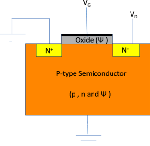
The MOSFET structure consists of a metal, oxide and semiconductor junction as shown below. The gate voltage can be used to modulate the conductivity of the device by altering the profiles of hole concentration (p), electron concentration (n) and potential (Ψ) in the device. The main governing equations in the device are drift-diffusion and Poisson’s equation.
Simulation Methodology
The device setup is shown below
Figure 1. MOSFET device shown along with the variables to be solved for in various domains
Equations to be solved for:-
1. Drift diffusion equation coupled with Poisson’s equation in the semiconductor domain,
2. Poisson’s equation in the gate oxide.
The above equations were solved using the equation based techniques in COMSOL .The drift diffusion and the Poisson’s equation governing the physics of the device had been framed to fit into the Coefficient form PDE interface in COMSOL. Appropriate initial values, boundary conditions, mesh size and solver configurations were chosen to yield proper results with reduced complexity in terms of time and memory.
Simulation Results and Discussion
The results obtained using the equation based approach were in conformity with those of the physics based model. Different profiles for p, n and Ψ were obtained for varying gate and drain voltages. The challenges faced were due to abrupt changes in p and n by orders of magnitude, a correct choice of initial values and boundary conditions, solver configurations and mesh sizes. The initial values of p and n were optimally chosen closer to the predicted solutions as their changes were highly abrupt. Proper adaptation of the sizes of mesh elements was important considering the abrupt changes of p and n profile in the semiconductor domain. Manipulation of solver configurations in terms of relative tolerance, number of iterations and damping factor was done to meet convergence criteria. During the dc sweep analysis of the gate voltage, an iterative technique of feeding the previously obtained solution as an initial value for the next study step was used to obtain convergent solution.
Conclusions
This paper summarizes the techniques used and challenges faced while solving the equation based model of MOSFET in COMSOL. This method will further be extended for the study of complicated MEMS structures where coupling between the semiconductor and beam mechanics equations will be demonstrated.
References
1. COMSOL Multiphysics example "DC Characteristics of a MOS Transistor (MOSFET)" model, version 3.5a.
2. COMSOL Multiphysics example “The KdV Equation and Solitons” model 5.4.
Acknowledgements
The authors would like to acknowledge IIT Madras for the provision of the licensed version of COMSOL Multiphysics tool for carrying out this work. The authors would also like to thank NNetRA for funding this work.