Modeling Nanowire Photovoltaic Devices
Introducing nanostructures into conventional III-V solar materials can improve the light capturing ability of solar devices. Nanowires are thin columns light absorbing material with such a small footprint that they can be grown epitaxially on lattice mismatched substrates. By growing III-V nanowires on standard Si substrates we can reduce reflection and increasing absorption through waveguiding effects.
We model the optical properties of these structures using the COMSOL® RF Module. The standard design of our model is a cylindrical nanowire on top of a square block of substrate. An array of nanowires is simulated by applying periodic boundary conditions. The material of the nanowire and substrate are assigned by specifying the frequency dependent index of refraction and attenuation coefficients. A port boundary is placed at the top of the structure to simulate incoming light. The light is weighted to the solar spectrum by specifying the incident power at each frequency.
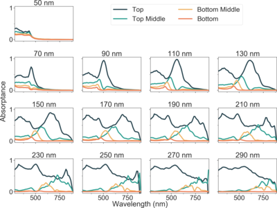
Previous work has shown that straight nanowires act as evanescent waveguides and are coupled to specific frequencies [1]. This results in peaks in the absorption spectrum where absorption is strong. By tuning the diameter of the nanowires and considering the incident power of the AM1.5 solar spectrum the straight, cylindrical nanowires can be optimized for photovoltaic applications [2]. We attempt to improve upon the cylindrical nanowire with straight sidewalls by introducing novel nanowire geometries such as tapering. We present an optimization study of tapered nanowire geometries and show its effects on the absorptance and total photocurrent generated by the nanowire structures. We show that by tapering the nanowire structure we can produce additional absorption events deeper within the nanowire structure than would be expected in a nanowire with straight sidewalls.
Download
- COMSOL_2020_Conference_P_Wilson.pdf - 0.42MB