

This blog post is your guide to building a simple and educational simulation app for designing a two-dimensional reflective metalens consisting of an array of glass nanopillars with varying diameters on a metal substrate. To build this app, we will use the Application Builder in the COMSOL Multiphysics® software. The app first finds the optimal metasurface parameters for a given wavelength and then computes the relationship between the nanopillar diameter and relative phase shift. Based on this, the app automatically builds the geometry for the metalens and, finally, runs a frequency-domain study on the finalized geometry to compute the electric field around the focus.
What Is a Metalens?
Over recent years, metamaterials have become a popular research topic in fields involving solutions of the wave equation, such as photonics and acoustics. A metamaterial is a composite material with an artificial structure (the structural unit is sometimes called a “meta-atom”) usually smaller than the wavelength. Because of this, metamaterials interact with electromagnetic fields like a homogeneous material with material properties that are distinct from those of the constituent materials. A mundane example of this is the grating in microwave-oven doors — a metal plate with air-filled holes is a metamaterial with a property that neither a solid metal plate nor air exhibit: it’s mostly transparent to short-wavelength visible light, while blocking completely long-wavelength microwaves.
In addition to potentially offering qualitative properties like no known “real” material does, the main advantage of metamaterials is that their properties can be tuned quantitatively — usually over a wide range — by changing the geometrical parameters of the structure. Many of the techniques developed for semiconductor manufacturing, such as photolithography, are applicable to making metametamaterials. Optical components made of such metamaterials are highly sought after for use in applications such as microscopy equipment and virtual reality technology.

A close-up of the grating in a microwave’s door.
In this blog post, we will focus on the reflective metalens: a flat array consisting of glass nanopillars on a metal substrate designed to work like a concave mirror. While it sounds like “metamirror” would be a more appropriate name, it’s important to appreciate the fact that the principle of operation of this device is not just conventional reflection but something known as anomalous reflection, where the reflected wave also undergoes a coordinate-dependent phase shift. A metalens has advantages compared to conventional optical devices such as lenses and mirrors, including:
- A metalens can be made a-fraction-of-a-micron thick, allowing miniaturization of optical devices
- A single metasurface can be designed to do much more than just focus light, so it’s possible to combine multiple conventional optical devices into one ultrathin metadevice
- Metamaterials can provide better performance for certain wavelength ranges, such as ultraviolet (UV)
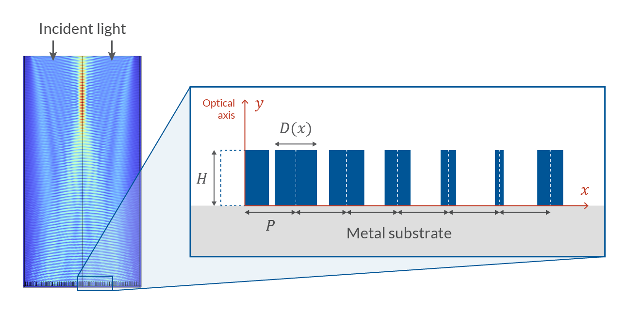
More specifically, we will consider a two-dimensional metalens consisting of silicon dioxide nanopillars of uniform height, H, and period, P, but varying diameter, D(x), placed on top of a flat metal substrate, as indicated in the figure below. For simplicity, we only consider a plane wave at normal incidence (moving in the negative y direction), polarized in the out-of-plane direction.
Mathematically speaking, a concave mirror is a device that, given an incident plane wave, shifts the wave’s phase locally such that it becomes a spherical wave converging at a point, i.e., the focus. Intuitively, we can imagine that as the thickness of the pillars is increased, the reflected wave picks up a larger phase shift due to the higher refractive index of the pillars compared to the surrounding air, but if we wish to build a functioning metalens, we need to obtain the precise quantitative relationship between the diameter and the relative phase shift \Delta \Phi (D), as described in the next section. The approach adopted here is based on Ref. 1.
Unit Cell Simulation
An efficient way to obtain \Delta \Phi (D) is to compute the phase shift due to a uniform periodic lattice, with all nanopillars having diameter D, and sweep over a range of diameter values. (You can learn more about modeling periodic structures here.) This allows us to use periodic boundary conditions so that we will only need to simulate a single unit cell of the lattice. Using a periodic port boundary condition to excite the incident wave means that we have convenient access to the phase shift of the wave through the argument of complex S-parameter S_{11}.
To build a functioning metalens, we need to be able to shift the local phase of the wave by any amount between 0 and 2\pi radians. Thus, we first need to find values of H, P, and the minimum and maximum diameter, D_\mathrm{min} and D_\mathrm{max}, such that \Delta \Phi ( D_\mathrm{max} ) – \Delta \Phi ( D_\mathrm{min} )=2 \pi, while retaining as high of a reflectance as possible. This is a frequency-domain optimization problem. The optimization step only requires results at the end points of the sweep, so we can cut out the intermediate steps, making the computation faster. Because we know that the narrower the pillars are, the wider the range of phase shifts, and that the smallest possible D_\mathrm{min} is governed by manufacturing limitations, we do not treat D_\mathrm{min} as a control parameter. Instead, D_\mathrm{min} is a fixed parameter with the value 20~\mathrm{nm} for most wavelengths (for wavelengths around 300~\mathrm{nm} and below, 10~\mathrm{nm} should be used instead to obtain good results). We are only interested in the relative phase, so our objective function should look something like
{S_{11}( D_\mathrm{min} )} \right]-2\pi\right|.
However, this expression is not ready for use in the user interface, as the software uses the sign convention e^{-iky} for a plane wave propagating in the positive y direction and defines the phase of a complex number from -\pi to \pi. When using COMSOL®’s sign convention, and after adding in the required operators to refer to the solutions for D=D_\mathrm{min} and D=D_\mathrm{max}, we end up with the expression shown in the figure below. We have also added a term involving the reflectances obtained from these two solutions to the Objective Function, which helps to avoid resonant modes and ensure high efficiency. If you would like to learn more about optimization, make sure to check out our blog post on shape optimization in electromagnetics or our on-demand course Performing Optimization in COMSOL Multiphysics®.

Settings used for the optimization study (Study 1). The optimization step uses the sweep results at the end points, so we need to place the Parametric Sweep step after the Optimization step, as shown in the Model Builder tree, and use the withsol() and sentind() operators to implement the desired objective function. We have also added a second expression for the reflectances to the Objective Function settings.
The only thing left to do is to run the full sweep with the optimized parameter values to obtain the phase shift for intermediate values between D_\mathrm{min} and D_\mathrm{max}. The result should look something like the figure below: a nice, monotonically increasing phase shift with high reflectance throughout the diameter range. Next, it’s time to build the metalens based on these results.

Plot of the results of the unit cell sweep for 400~\mathrm{nm}, demonstrating a phase shift that increases monotonically from 0 to 2\pi while retaining a high reflectance throughout the nanopillar diameter range.
Metalens Simulation
Before we can build the metalens geometry, we need to transform the phase shift function \Delta \Phi (D) into a nanopillar diameter distribution function D(x), where x is the distance from the optical axis. We know that an ideal focusing mirror applies the following phase shift to a plane wave at normal incidence:
Here, f and R are the focal length and the radius of the metalens, respectively. For convenience, we have chosen to define \Delta \phi (x) such that \Delta \phi (R) =0. The rest is a matter of a few numerical manipulations: assuming that the phase shift is monotonic, we can invert \Delta \Phi (D) to obtain \Delta \Phi ^{-1} (\phi) \equiv D( \phi ), add periodicity so that D( \phi \pm 2n\pi ) =D( \phi ), and form a composite function with \Delta \phi (x) so that we end up with D(\phi(x)) \equiv D(x) . An example of what this should look like is shown in the figure below.

Nanopillar diameter distribution D(x) as a function of distance away from the optical axis of the metalens with focal length 25~\mu\mathrm{m}, radius 7.5~\mu\mathrm{m}, and operating wavelength of 400~\mathrm{nm}.
The next challenge is to convert this function into an actual geometry. If we define the abovementioned functions in the Global Definitions node, we can define the nanopillar as a geometry part with the pillar position x as an input and with the width set equal to D(x). We then just need to add \lfloor R/P \rfloor (here, R is the radius of the metalens and P is the metasurface period) instances of this part to the geometry sequence. Better still, we can use the Application Builder to write a method that does this for us, as discussed in the next section.
About the App Implementation
Let’s first take a look at how to automate generating the metalens geometry. In essence, in the Application Builder, we can use the method model.component(<comp>).geom(<geom>).create(<name>, "PartInstance") to create a geometry part instance and then set the input parameters using model.component(<comp>).geom(<geom>).feature(<name>).setEntry. Placing these commands inside a for loop will get us the entire metasurface. It should be noted that this approach works well for small metalenses (R/P\lesssim100) and for educational purposes. For large metalenses, it is necessary to use a hierarchical submodeling approach where the COMSOL® model is used to compute the unit cell response for varying geometry parameters and where the result is used as part of a larger program using Java® methods or LiveLink™ for MATLAB®. Now that we got a taste of writing methods, we can create a button that takes the output of the initial optimization using
("inputexpr", <expr-name>, <val>)model.result().numerical("gev1").getReal() and sets the model parameters to these values using model.param().set(). Additionally, we used setRibbonItemEnabled() to enable the button for the next step only after the previous ones are completed.
The Application Builder makes it possible to achieve much more than just automating the more tedious steps in the design process. For instance, packaging the model into an app means that we can create a custom user interface (UI), which can be highly beneficial since the user will be able to monitor the entire design process at a glance. The figure below shows the UI of the app. As a possible next step you can of course use COMSOL Compiler™ to create a standalone app.

The UI of the metalens app, designed so that all aspects of the design process can be monitored at a glance.
A screen recording of the metalens app in action.
Concluding Thoughts
In this blog post we summarized how to build an app that can be used to design a two-dimensional reflective metalens with specified size, focal length, and operation wavelength. We saw that by using the Application Builder in COMSOL Multiphysics®, the relatively involved design process can be streamlined with a UI that enables the user to conveniently monitor the design process from start to finish.
However, we have barely scratched the surface of metalens design. Further extensions include considering three-dimensional lenses, including lens performance analysis (e.g., the size of focus and dispersion properties, as analyzed in Ref. 1), and including multiphysics to model thermally configurable metalenses like in Ref. 2. We hope to explore some of these more advanced topics in a future blog post.
Next Steps
Try out the metalens app yourself by clicking the button below, which will take you to the Application Gallery:
References
- H. Guo et al., “Design of Polarization-Independent Reflective Metalens in the Ultraviolet–Visible Wavelength Region,” Nanomaterials, vol. 11, no. 5, 2021; https://doi.org/10.3390/nano11051243.
- A. Archetti et al., “Thermally reconfigurable metalens,” Nanophotonics, vol. 11, no. 17, pp. 3969–3980, 2022; https://doi.org/10.1515/nanoph-2022-0147.
Oracle and Java are registered trademarks of Oracle and/or its affiliates. MATLAB is a registered trademark of The MathWorks, Inc.


Comments (3)
Marco Gandolfi
November 10, 2023Thank you very much for the useful post. What are the boundary conditions used on the lateral sides of the complete metalens simulation (i.e. the boundary conditions used to achieve the results reported in the right panel of the screenshots)? In this simulation, is the light introduced with a port from the top boundary? Is this port user defined? Do you use a plane wave? Thank you for your attention.
Ville Paasonen
November 12, 2023 COMSOL EmployeeHello Marco,
I used a PML (Perfectly Matched Layer) at the lateral sides of the full metalens simulation, and a Scattering Boundary Condition at the top boundary for the incident plane wave (polarized in the out-of-plane direction). The Port Boundary Condition was used only in the unit cell simulation.
Marco Gandolfi
November 14, 2023Thank you very much for your reply.
Now it’s ok.
Best Regards