The Application Gallery features COMSOL Multiphysics® tutorial and demo app files pertinent to the electrical, structural, acoustics, fluid, heat, and chemical disciplines. You can use these examples as a starting point for your own simulation work by downloading the tutorial model or demo app file and its accompanying instructions.
Search for tutorials and apps relevant to your area of expertise via the Quick Search feature. Note that many of the examples featured here can also be accessed via the Application Libraries that are built into the COMSOL Multiphysics® software and available from the File menu.

This simple model demonstrates how to use the Semiconductor Optoelectronics interfaces to model a simple GaAs PIN diode structure. Both the stimulated and spontaneous emission in the semiconductor are accounted for. The corresponding absorption of the light and the associated change in ... Read More
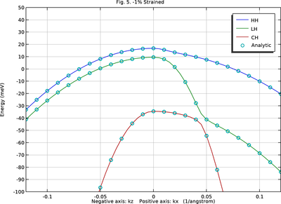
This benchmark model computes the valence band structure of an unstrained and a strained bulk GaN wurtzite crystal, as a tutorial for users who wish to set up multiple wave function components with the Schrödinger Equation interface. The model follows the formulation given in the ... Read More
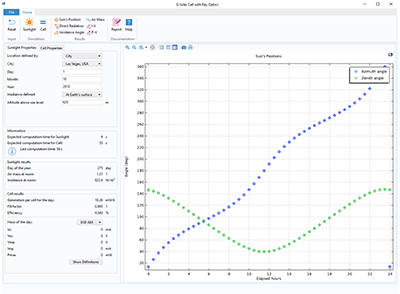
This app demonstrates the following: Multiple components (1D and 3D) in a single app Using the same choice list in the app as in the model using Data Access functionality Output numerical results for a specific time step using a combo box The app combines the Ray Optics Module and ... Read More

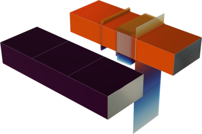
In this first half of a two-part example, a 2D model of a trench-gate IGBT is built, which will be extended to 3D in the second half. In general, it is the most efficient to start with a 2D model to make sure everything works as expected, before extending it to 3D. The Caughey&ndash ... Read More

The metal-silicon-oxide (MOS) structure is the fundamental building block for many silicon planar devices. Its capacitance measurements provide a wealth of insight into the working principles of such devices. This tutorial constructs a simple 1D model of a MOS capacitor (MOSCAP). Both ... Read More
In a diode or a transistor, when a p-n junction is reverse-biased (the p-side is connected to a lower potential than the n-side), ideally, no current should flow. However, due to minority carriers (electrons in the p-side and holes in the n-side), a small current, known as the reverse ... Read More

MOSFETs typically operate in three regimes depending on the drain-source voltage for a given gate voltage. Initially the current-voltage relation is linear, this is the Ohmic region. As the drain-source voltage increases the extracted current begins to saturate, this is the saturation ... Read More

This benchmark model simulates three different heterojunction configurations under forward and reverse bias. It shows the difference in using the continuous quasi-Fermi level formulation versus the thermionic emission formulation for the charge transfer across the heterojunction. The ... Read More

This model simulates a GaN based light emitting diode. The emission intensity, spectrum, and quantum efficiency are calculated as a function of the driving current. Direct radiative recombination across the band gap is modeled, as well as non-radiative Auger and trap-assisted ... Read More
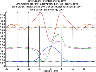
The double barrier structure is of interest because of its application in semiconductor devices such as resonant-tunneling diodes. This verification example demonstrates the Schrödinger Equation interface to set up a simple 1D GaAs/AlGaAs double barrier structure to analyze the ... Read More