

We often want to model an electromagnetic wave (light, microwaves) incident upon periodic structures, such as diffraction gratings, metamaterials, or frequency selective surfaces. This can be done using the RF or Wave Optics modules from the COMSOL product suite. Both modules provide Floquet periodic boundary conditions and periodic ports and compute the reflected and transmitted diffraction orders as a function of incident angles and wavelength. This blog post introduces the concepts behind this type of analysis and walks through the set-up of such problems.
The Scenario
First, let’s consider a parallelepided volume of free space representing a periodically repeating unit cell with a plane wave passing through it at an angle, as shown below:

The incident wavevector, \bf{k}, has component magnitudes: k_x = k_0 \sin(\alpha_1) \cos(\alpha_2), k_y = k_0 \sin(\alpha_1) \sin(\alpha_2), and k_z = k_0 \cos(\alpha_1) in the global coordinate system. This problem can be modeled by using Periodic boundary conditions on the sides of the domain and Port boundary conditions at the top and bottom. The most complex part of the problem set-up is defining the direction and polarization of the incoming and outgoing wave.
Defining the Wave Direction
Although the COMSOL software is flexible enough to allow any definition of base coordinate system, in this posting, we will pick one and use it throughout. The direction of the incident light is defined by two angles, \alpha_1 and \alpha_2; and two vectors, \bf{n}, the outward pointing normal of the modeling space and \bf{a_1}, a vector in the plane of incidence. The convention we choose here is to align \bf{a_1} to the global x-axis and align \bf{n} with the global z-axis. Thus, the angle between the wavevector of the incoming wave and the global z-axis is \alpha_1, the elevation angle of incidence, where -\pi/2 > \alpha_1 > \pi/2 with \alpha_1 = 0, meaning normal incidence. The angle between the incident wavevector and the global x-axis is the azimuthal angle of incidence, \alpha_2, which lies in the range, -\pi/2 > \alpha_2 \geq \pi/2. As a consequence of this definition, positive values of both \alpha_1 and \alpha_2 imply that the wave is traveling in the positive x- and y-direction.
To use the above definition of direction of incidence, we need to specify the \bf{a_1} vector. This is done by picking a Periodic Port Reference Point, which must be one of the corner points of the incident port. The software uses the in-plane edges coming out of this point to define two vectors, \bf{a_1} and \bf{a_2}, such that \bf{a_1 \times a_2 = n}. In the figure below, we can see the four cases of \bf{a_1} and \bf{a_2} that satisfy this condition. Thus, the Periodic Port Reference Point on the incoming side port should be the point at the bottom left of the x-y plane, when looking down the z-axis and the surface. By choosing this point, the \bf{a_1} vector becomes aligned with the global x-axis.

Now that \bf{a_1} and \bf{a_2} have been defined on the incident side due to the choice of the Periodic Port Reference Point, the port on the outgoing side of the modeling domain must also be defined. The normal vector, \bf{n}, points in the opposite direction, hence the choice of the Periodic Port Reference Point must be adjusted. None of the four corner points will give a set of \bf{a_1} and \bf{a_2} that align with the vectors on the incident side, so we must choose one of the four points and adjust our definitions of \alpha_1 and \alpha_2. By choosing a periodic port reference point on the output side that is diametrically opposite the point chosen on the input side and applying a \pi/2 rotation to \alpha_2, the direction of \bf{a_1} is rotated to \bf{a_1'}, which points in the opposite direction of \bf{a_1} on the incident side. As a consequence of this rotation, \alpha_1 and \alpha_2 are switched in sign on the output side of the modeling domain.

Next, consider a modeling domain representing a dielectric half-space with a refractive index contrast between the input and output port sides that causes the wave to change direction, as shown below. From Snell’s law, we know that the angle of refraction is \beta=\arcsin \left( n_A\sin(\alpha_1)/n_B \right). This lets us compute the direction of the wavevector at the output port. Also, note that this relationship holds even if there are additional layers of dielectric sandwiched between the two half-spaces.
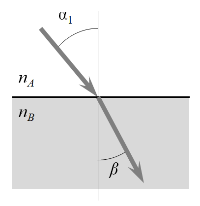
In summary, to define the direction of a plane wave traveling through a unit cell, we first need to choose two points, the Periodic Port Reference Points, which are diametrically opposite on the input and output sides. These points define the vectors \bf{a_1} and \bf{a_2}. As a consequence, \alpha_1 and \alpha_2 on the input side can be defined with respect to the global coordinate system. On the output side, the direction angles become: \alpha_{1,out} = -\arcsin \left( n_A\sin(\alpha_1)/n_B \right) and \alpha_{2,out}=-\alpha_2 + \pi/2.
Defining the Polarization
The incoming plane wave can be in one of two polarizations, with either the electric or the magnetic field parallel to the x-y plane. All other polarizations, such as circular or elliptical, can be constructed from a linear combination of these two. The figure below shows the case of \alpha_2 = 0, with the magnetic field parallel to the x-y plane. For the case of \alpha_2 = 0, the magnetic field amplitude at the input and output ports is (0,1,0) in the global coordinate system. As the beam is rotated such that \alpha_2 \ne 0, the magnetic field amplitude becomes (-\sin(\alpha_2), \cos(\alpha_2),0). For the orthogonal polarization, the electric field magnitude at the input can be defined similarly. At the output port, the field components in the x-y plane can be defined in the same way.

So far, we’ve seen how to define the direction and polarization of a plane wave that is propagating through a unit cell around a dielectric interface. You can see an example model of this in the Model Gallery that demonstrates an agreement with the analytically derived Fresnel Equations.
Defining the Diffraction Orders
Next, let’s examine what happens when we introduce a structure with periodicity into the modeling domain. Consider a plane wave with \alpha_1, \alpha_2 \ne 0 incident upon a periodic structure as shown below. If the wavelength is sufficiently short compared to the grating spacing, one or several diffraction orders can be present. To understand these diffraction orders, we must look at the plane defined by the \bf{n} and \bf{k} vectors as well as in the plane defined by the \bf{n} and \bf{k \times n} vectors.

First, looking normal to the plane defined by \bf{n} and \bf{k}, we see that there can be a transmitted 0th order mode with direction defined by Snell’s law as described above. There is also a 0th order reflected component. There also may be some absorption in the structure, but that is not pictured here. The figure below shows only the 0th order transmitted mode. The spacing, d, is the periodicity in the plane defined by the \bf{n} and \bf{k} vectors.

For short enough wavelengths, there can also be higher-order diffracted modes. These are shown in the figure below, for the m=\pm1 cases.

The condition for the existence of these modes is that:
for: m=0,\pm 1, \pm 2,…
For m=0 , this reduces to Snell’s law, as above. For \beta_{m\ne0}, if the difference in path lengths equals an integer number of wavelengths in vacuum, then there is constructive interference and a beam of order m is diffracted by angle \beta_{m}. Note that there need not be equal numbers of positive and negative m-orders.
Next, we look along the plane defined by the \bf{n} and \bf{k} vectors. That is, we rotate our viewpoint around the z-axis such that the incident wavevector appears to be coming in normally to the surface. The diffraction into this plane are indexed as the n-order beams. Note that the periodic spacing, w, will be different in this plane and that there will always be equal numbers of positive and negative n-orders.

COMSOL will automatically compute these m,n \ne 0 order modes during the set-up of a Periodic Port and define listener ports so that it is possible to evaluate how much energy gets diffracted into each mode.
Last, we must consider that the wave may experience a rotation of its polarization as it gets diffracted. Thus, each diffracted order consists of two orthogonal polarizations, the In-plane vector and Out-of-plane vector components. Looking at the plane defined by \bf{n} and the diffracted wavevector \bf{k_D}, the diffracted field can have two components. The Out-of-plane vector component is the diffracted beam that is polarized out of the plane of diffraction (the plane defined by \bf{n} and \bf{k}), while the In-plane vector component has the orthogonal polarization. Thus, if the In-plane vector component is nonzero for a particular diffraction order, this means that the incoming wave experiences a rotation of polarization as it is diffracted. Similar definitions hold for the n \ne 0 order modes.
![]()
Consider a periodic structure on a dielectric substrate. As the incident beam comes in at \alpha_1, \alpha_2 \ne 0 and there are higher diffracted orders, the visualization of all of the diffracted orders can become quite involved. In the figure below, the incoming plane wave direction is shown as a yellow vector. The n=0 diffracted orders are shown as blue arrows for diffraction in the positive z-direction and cyan arrows for diffraction into the negative z-direction. Diffraction into the n \ne 0 order modes are shown as red and magenta for the positive and negative directions. There can be diffraction into each of these directions and the diffracted wave can be polarized either in or out of the plane of diffraction. The plane of diffraction itself is visualized as a circular arc. Note that the plane of diffraction for the n \ne 0 modes is different in the positive and negative z-direction.

All of the ports are automatically set up when defining a periodic structure in 3D. They capture these various diffracted orders and can compute the fields and relative phase in each order. Understanding the meaning and interpretation of these ports is helpful when modeling periodic structures.


Comments (15)
Bryan Adomanis
March 21, 2014Great explanation, Walter! You should lobby to have it put in the documentation!
Aneesh M Joseph
March 31, 2014subject: problem in assigning diffraction orders for 2d nano pillar grating structure in comsol 3d modeling
Can you help me in this regard?
I would like to find the electric filed intensity of reflection(or reflectance) from gold nano pillars from gold substrate, with the consideration of diffraction orders in case of reflection((1,1 ), (1,0 )reflection grating orders), for the different wave lengths starting from 200 nm to 1000 nm, for a fixed angle of incidence (normal incidence, or 30 degree angle of incidence)
I had made a 2D grating structures in 3D modeling Wizard of Comsol 4.4 version, While I am putting Diffraction orders( m=0, n=0 ; m=-1, n=0 ; m=+1, n=0) with “port reference points” as diagonally opposite end of Unit square cell with periodic boundary conditions on all four sides( by doing copay face). Unfortunately it gives me zero electric filed while i am running., If I run the same model without diffraction order it gives the result but only from one order diffraction (normal reflection) . Since I need to calculate reflection from at least two orders (0 th order and 1 st order) I have to include those diffraction orders to my model
Can you help me in this regard?
can you tell me how to put diffraction orders (with proper port reference points)in 2d grating on 3D model?
Also How can i implement PML layer over the port ( or it is really needed ), since if i add PMLl layer on the top of port, selecting port reference point is declined by default. I follow the pyramidal absorption model for making the infinite array of my 2d Grating nano structures( there a PML layer added over the port)
the plasmonic wire grating model available in Comsol library is just a 2D model , so we can’t able to follow the same thing in here in our model.
I used this blog for making port reference points and putting periodic ports
http://www.comsol.co.in/blogs/modeling-electromagnetic-waves-periodic-structures/
Please help me in this regard..
Thank you
Aneesh M Joseph
Illia Fedorin
November 5, 2014Great work, Walter!!
If you have some example models it would be great to see (.mph as an example).
Thanks in advance!
Illia Fedorin.
Walter Frei
November 7, 2014 COMSOL EmployeeDear Illia,
Right now the plasmonic wire grating example is the best place to get started: http://www.comsol.com/model/10032
And we are working on some other models as well.
Best,
Walter
Jalpa Soni
March 31, 2015Hello everyone …
Can anyone help me How to use Floquet boundary condition in case of 3d structure. I want to simulate a model which calculate scattering through array of nanodisc which lie on XY plane .. say i am supposed to incident an electric field through z- axis polarization along either x or y. So in that case what should be my floquet boundary condition??
Walter Frei
March 31, 2015 COMSOL EmployeeWe do recommend that you study the examples in our model library which demonstrate Floquet periodicity. The following examples are helpful:
http://www.comsol.com/model/10032 (RF Module)
http://www.comsol.com/model/14705 (Wave Optics Module, same example)
This demonstrates the diffraction orders (in 2D)
In 3D:
http://www.comsol.com/model/frequency-selective-surface-periodic-complementary-split-ring-resonators-15711
http://www.comsol.com/model/modeling-of-pyramidal-absorbers-for-an-anechoic-chamber-12129
http://www.comsol.com/model/fresnel-equations-12407
These demonstrate Floquet periodicity, but without the computation of diffraction orders.
Kalpana Singh
April 1, 2015Hello Walter
From last 6 months, I have been trying to learn COMSOL Multiphysics. I couldn’t find anyone to discuss my doubts while doing the tutorials for Plasmonic wire grating and FSS , split ring resonator. I finally found this blog where periodic structure is discussed as my work is also on periodic structures. Writing my questions here hoping that would be answered by you or anyone who will read this.
While going through the FSS/Split ring resonator I have following doubts:
1) the (1) emw.k0*sin(theta)*cos(phi) (2) emw.k0*sin(theta)*sin(phi) (3) emw.k0*cos(phi) are put in variables. Can we write them in parameters? And I think these components determine the direction of incident of light.
2)Difference between domain backed and PEC slit type. What actually their functions are and how would they affect the simulation?
3)Port orientation is been taken as reverse for both ports 1 and 2. Why? And the directions of the arrow of the port is same whether I click it for forward or reverse. What does it make difference?
4) While defining the properties of port, input quantity is given as magnetic field. Why it is magnetic field, can’t we put electric field as a input quantity ? And also exp(-i*k_x*x)*exp(-i*k_y*y) j A/m is given for the mode, it means wave is traveling in XY plane K has both the component kx and ky and the direction of magnetic field is along y direction. but magnetic field should be perpendicular to direction of propagation.
4) again if wave is propagating in XY plane than how the propagation constant beta = abs(k_z)?
5) Since both plasmonic wire and FSS are periodic structure then why port periodicity is considered in former one not in later one?
I am lost. Please help me out.
Thanks
Kalpana
Walter Frei
April 1, 2015 COMSOL EmployeeDear Kalpana,
The appropriate place to ask such questions would be of your COMSOL Support Team: http://www.comsol.com/support/
Abhishek Kumar
December 12, 2015Hello Walter
Well by looking at your post I tried to create a model which calculate the transmission through periodic structure which is fabricated on ITO coated glass substrate.
I have used periodic port to ensure that it would capture the information about all diffraction order.
Also I have used the concept of Frequency selctive model from RF module. I have some doubt in this model why there Port type is Domain-backed and orientation is Reverse.
ahmed mansour
July 9, 2016Hi all
Does anybody knows how to set perfectly matched layer (PML) in boundary condition in electromagnetic wave time domain (teew)
Walter Frei
July 11, 2016 COMSOL EmployeeHello Ahmed,
You may find this article helpful:
https://www.comsol.com/blogs/using-perfectly-matched-layers-and-scattering-boundary-conditions-for-wave-electromagnetics-problems/
As for time-domain modeling, for this you will currently want to use the absorbing BC.
Ahmed Mansour
July 17, 2016hi walter
i want to know, do comsol FDTD method for simulation spectral thermal radiation in subwavelength .However, beware that the time solver is not in the best equipped form. Lack of PMLs and any built-in support for metals
Khoa Phan
August 20, 2016Can someone give me a guide on what is the periodic condition: continuity and Floquet? Also, in Floquet periodicity, there are two choices for vector kF: User define and From port period.
Imran Moez Khan
March 29, 2019Hi Walter,
Not sure if you’d see this comment because its on such an old post, but thanks a lot for this write-up! – really comprehensive description of how the physics model is built for this boundary condition.
I just found this part a bit unclear: “Last, we must consider that the wave may experience a rotation of its polarization as it gets diffracted. Thus, each diffracted order consists of two orthogonal polarizations, the In-plane vector and Out-of-plane vector components.”
Given we were talking about the n x k and n x (n x k) planes – I’m not sure if I am correct about this – but I imagine the polarization rotation only occurs in the n x (n x k) plane rather than the n x k plane, since in the n x k plane there wouldn’t be a change in the alpha2 of the diffracted wave?
Aditya Sengupta
January 4, 2023Hello Walter,
I wish to simulate TEM mode analysis on a waveguide, but I don’t have the RF module in my University’s class kit. Is there a way to simulate it on the Wave Optics module?