

Accurate modeling of semiconductor manufacturing processes can require detailed geometries, fine meshes, and coupled physics. While simplification can reduce computational demands, sufficient physical detail must be retained to capture physical behavior. In this blog post, we discuss how NVIDIA-accelerated computing can reduce computation time for high-fidelity semiconductor manufacturing simulations.
Accelerating Multiphysics Simulation with NVIDIA cuDSS
The NVIDIA CUDA Direct Sparse Solver (cuDSS) is fully integrated into the standard solver framework of COMSOL Multiphysics®. With this integration, the software can leverage the high memory bandwidth and massive parallel architecture of NVIDIA GPUs for multiphysics analysis. GPU acceleration can substantially speed up the solution of large sparse linear systems, including those that arise repeatedly in nonlinear iterations, implicit time-stepping methods, and continuation methods used in parametric studies. By speeding up the linear system solves at each iteration or time step, NVIDIA cuDSS can improve overall simulation performance.
Nonlinear and time-dependent studies are common in semiconductor modeling, including modeling of applications involving electrokinetics, electromagnetics, and fluid dynamics. GPU acceleration can reduce the runtime of such studies from overnight to just a few hours. For example, for the mechanical polishing benchmark model discussed here, using two GPUs accelerated the runtime from 14–16 hours on the tested CPU configurations to just 2 hours and 9 minutes. Similarly, early benchmark tests on the photoresist spin-coating model presented here showed an approximately 92% lower runtime compared with the tested Intel® Xeon Gold configuration. Below is a more detailed look at these and other benchmark semiconductor models that show similar speedups thanks to GPU acceleration.
NVIDIA cuDSS Semiconductor Benchmarks in COMSOL
Model: Simulation of the Flow Field and Abrasive Particles in Chemical Mechanical Polishing Equipment
Model: Simulation of the Flow Field and Abrasive Particles in Chemical Mechanical Polishing Equipment
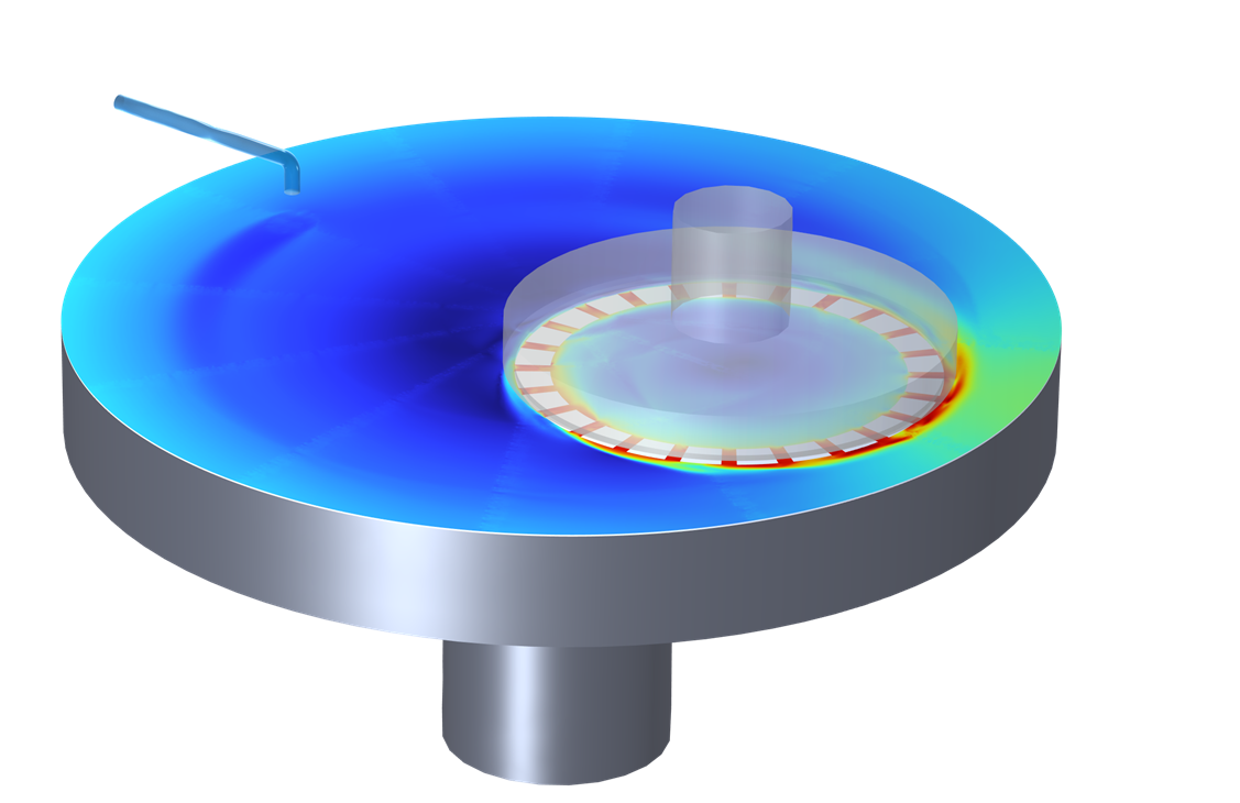 Model geometry of the chemical mechanical polishing (CMP) process, where the wafer is positioned on the polishing head and pressed onto the larger disc of fluid.
CMP is a crucial technique for surface planarization that is widely used in semiconductor fabrication. This model simulates the flow field around the wafer and tracks the motion of abrasive particles carried by the flow. The strongly coupled physics and many degrees of freedom make this a very computationally demanding model. With NVIDIA cuDSS, the model ran more than 6× faster than on the tested CPU configurations, allowing it to be solved and adjusted several times throughout a workday, whereas the CPU-based solvers would need more than a full workday just to run once.
|
Configuration |
Hardware |
Runtime |
|---|---|---|
|
2 GPUs |
GPU |
2 h 9 m |
|
Intel® Xeon Gold, 12 cores |
CPU |
13 h 44 m |
|
Intel® Xeon 6, 12 cores |
CPU |
16 h 28 m |
Model: Electrodeposition of a Microconnector Bump with Deforming Geometry in 3D
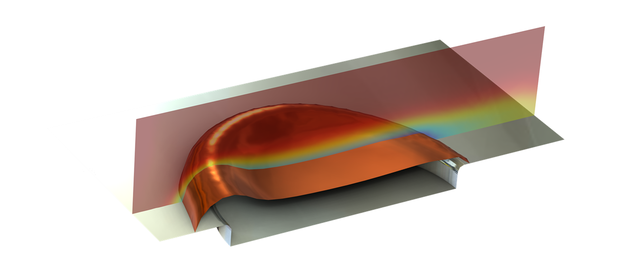 Model geometry of a microconnector bump, a common feature of chips that are bonded directly onto substrates using bumps and underfill.
This model simulates the evolution of a microconnector bump over time as copper deposits onto an electrode surface. Cupric ions are transported through the electrolyte by convection and diffusion, and the electrode kinetics are described by a concentration-dependent Butler–Volmer expression. The coupling of electrochemistry, fluid flow, and deformed geometry makes for a sizeable computational load, which NVIDIA cuDSS handled more than 2× faster than the conventional CPU solvers.
|
Configuration |
Hardware |
Runtime |
|---|---|---|
|
1 GPU |
GPU |
7 m 47 s |
|
Intel® Xeon Gold, 12 cores |
CPU |
17 m 16 s |
|
Intel® Xeon 6, 12 cores |
CPU |
17 m 46 s |
Model: Copper Deposition in a Trench Using the Phase-Field Method
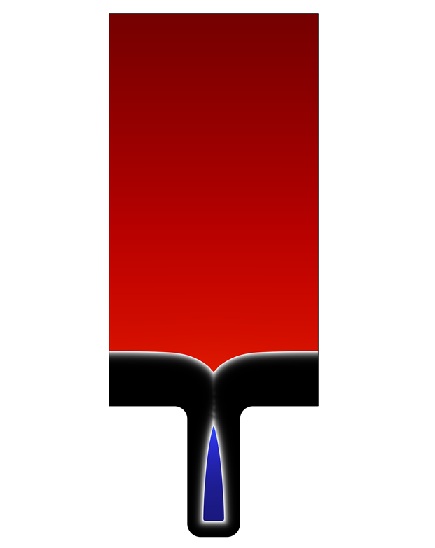
2D model geometry of a “trench” that causes uneven copper deposition.
During copper deposition, narrow regions can lead to nonuniform plating and the formation of voids, as shown by the blue area in the 2D geometry. The model captures this effect by coupling ion transport and electrode reactions with a phase field formulation based on the Cahn–Hilliard equation, where it tracks the evolving shape of the copper deposit. The benchmark demonstrates that even for a more lightweight model, NVIDIA cuDSS can significantly outperform conventional CPU solvers, in this case running more than 2× faster.
|
Configuration |
Hardware |
Runtime |
|---|---|---|
|
1 GPU |
GPU |
1 m 59 s |
|
Intel® Xeon Gold, 12 cores |
CPU |
4 m 51 s |
|
Intel® Xeon 6, 12 cores |
CPU |
4 m 51 s |
Model: Photoresist Spin Coating
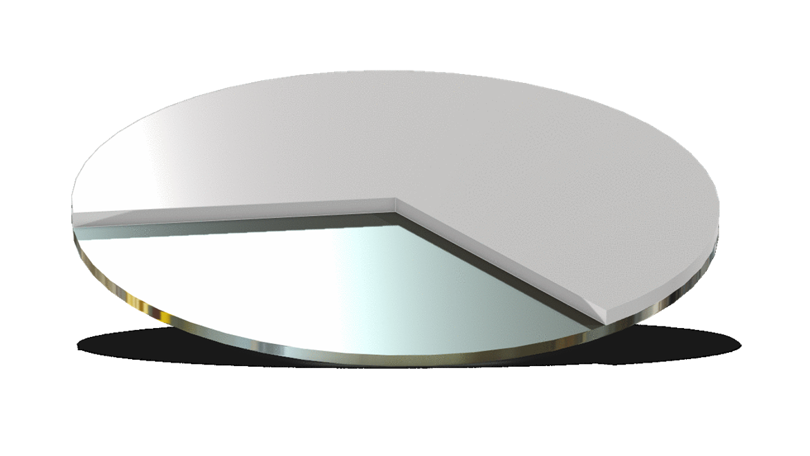 The model geometry of a photoresist coating on top of a substrate.
Photoresist coating is an important process in semiconductor manufacturing where the thickness of the photoresist layer needs to be precisely controlled. Usually, the photoresist layer is thinned by spin coating, where centrifugal force is used to throw excess photoresist away from the wafer surface until a specific thickness is achieved. This model simulates the process using swirl flow to calculate the film thickness at different viscosities and rotational speeds. NVIDIA cuDSS substantially reduced the runtime for this model, achieving a speedup of up to 13× compared with the CPU-based solvers.
|
Configuration |
Hardware |
Runtime |
|---|---|---|
|
1 GPU |
GPU |
1 m 28 s |
|
Intel® Xeon Gold, 12 cores |
CPU |
19 m 27 s |
|
Intel® Xeon 6, 12 cores |
CPU |
16 m 17 s |
Model: Electrostatic Discharge Test of a PCB
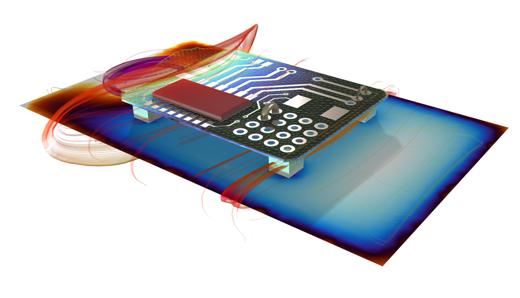 A PCB mounted on a copper ground plane being subjected to electrostatic discharge (ESD) events.
PCBs are subject to ESD events that can cause malfunctions or logical errors. ESD testing helps engineers assess whether electronic assemblies can withstand specified discharge conditions. Numerical simulation can identify ESD problems during the design stage while providing detailed electromagnetic field distributions that are difficult or even impossible to measure accurately in the real world. ESD currents are highly nonlinear, which makes the ESD testing model a good candidate for GPU acceleration. In this case, NVIDIA cuDSS achieved a speedup of about 3× compared to the tested CPU configurations.
|
Configuration |
Hardware |
Runtime |
|---|---|---|
|
2 GPUs |
GPU |
1 m 49 s |
|
Intel® Xeon Gold, 12 cores |
CPU |
5 m 21 s |
|
Intel® Xeon 6, 12 cores |
CPU |
5 m 48 s |
Model: Residual Stress and Warpage Due to the Curing of the Underfill in a Chip Package
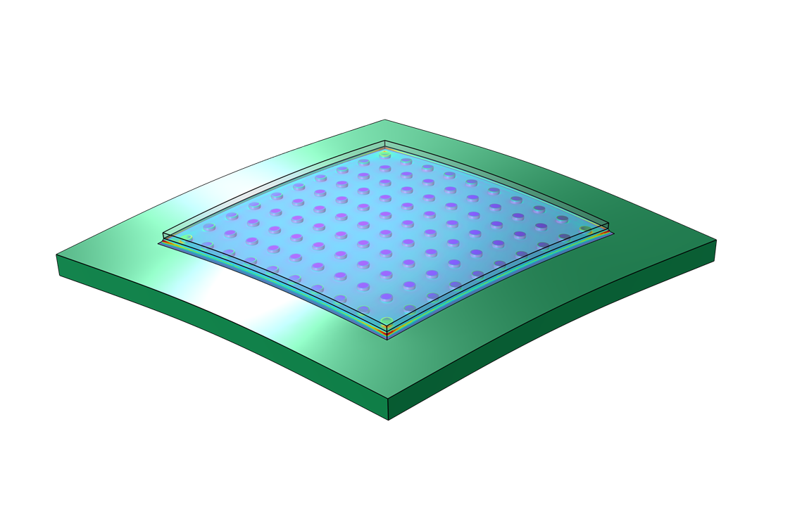 Model geometry of a flip chip (FC), a widely used form of semiconductor packaging where the chip is directly bonded to the substrate using bumps and a polymer underfill that fills the gap between bumps and substrate.
FC packaging allows for high interconnection density as well as a reduction in package size, but the different thermal expansion properties of the materials involved may cause warpage of the package during underfill curing. This model simulates the warpage of the chip package throughout the curing process as the package is exposed to different thermal conditions. NVIDIA cuDSS reduced the runtime substantially, with a speedup of more than 6× compared to the tested CPU configurations.
|
Configuration |
Hardware |
Runtime |
|---|---|---|
|
1 GPU |
GPU |
6 m 20 s |
|
Intel® Xeon Gold, 12 cores |
CPU |
38 m 36 s |
|
Intel® Xeon 6, 12 cores |
CPU |
48 m 39 s |
Learn More About GPU Acceleration in COMSOL®
By accelerating multiphysics simulations with NVIDIA cuDSS, the COMSOL® software helps engineers evaluate more process and design options in less time — from copper deposition and photoresist coating to package warpage and polishing equipment. Faster simulation supports shorter development cycles and more informed engineering decisions before physical testing. To hear more about the capabilities of NVIDIA-accelerated computing support for semiconductor applications, reach out to your local COMSOL representative.




Comments (0)