
Chemical vapor deposition (CVD) is used in almost all semiconductor manufacturing processes, and most modern electronics would not exist without it. Notably, this process is used to produce uniformly thin films for microchips. Additional processes that incorporate CVD include corrosion prevention, glass coating, and the production of synthetic diamonds. In this blog post, we’ll give a brief introduction to CVD and look at a boat reactor model example to show how modeling can provide more insight into this process.
What Is CVD?
In CVD, a solid substrate is placed in a reaction chamber filled with a gas mixture that contains precursor chemicals. This is a reactive process, thus distinguishing it from physical processes like evaporation and sputtering. There are several different CVD methods, each of which uses different chemistries, substrate materials, and temperatures. Depending on the operating conditions, there are various types of CVD reactors, such as plasma-enhanced, atmospheric pressure, low-pressure, and ultrahigh vacuum CVD reactors.
Low-pressure reactors, such as a boat reactor, operate in subatmospheric pressures and are typically used in the CVD process for higher diffusivity of the gaseous species and to eliminate unwanted gas-phase reactions. This results in deposition of a layer with uniform thickness, as the process becomes limited by the deposition kinetics. This makes the boat reactor a suitable candidate for chip manufacturing, where the deposition of a thin, uniform silicon layer is desired.
A typical boat reactor consists of the following components:
- A boat-shaped container made of quartz or silicon to hold the wafer to be coated
- An inlet for the precursor chemicals to be introduced into the reaction chamber
- A heat source to provide the required temperature for the reaction to occur
- A substrate on which the desired material is to be deposited
- An outlet for the residual gases to exit the reactor
A schematic of a boat reactor can be seen below.
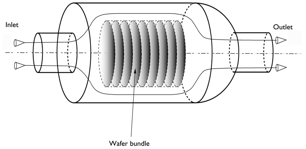 A typical low-pressure CVD boat reactor setup.
The reactant gas, which is silane (SiH4) in this case, enters the reactor from the inlet and reacts on the wafer bundle to form hydrogen and silicon. The remaining mixture leaves the reactor through the outlet. The silicon deposition on the wafers is directly proportional to the concentration of silane in the incoming gaseous mixture.
Let’s now look at the different parts of a boat reactor model, created with the COMSOL Multiphysics® software.
Overview of the Model Components
The modeled domain of the boat reactor can be seen in the figure below. The domain is simplified by considering a 2D axisymmetric geometry, and the wafer bundle is modeled as an anisotropic porous medium that only permits radial transport, used for computational efficiency. The temperature in the CVD reactor is assumed to be constant.
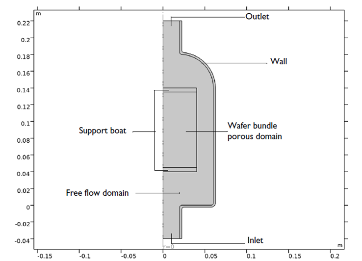 The domain of the boat reactor modeled in COMSOL Multiphysics®.
The goal of the example model is to describe the rate of deposition as a function of the fluid mechanics and kinetics in such a system. The model couples the momentum and mass transport with the reaction kinetics for the desired deposition process. Accordingly, the following three physics phenomena are accounted for:
- Chemistry
- Fluid flow
- Mass transport
Below, you will find more details on these phenomena.
Chemistry
First, let’s consider the chemistry. The main precursor chemical in the model is silane gas. The gas enters the reactor through the inlet, resulting in the deposition of solid silicon on the wafer bundle. This reaction can be described as follows:
Here, the reactant gas is diluted in inert nitrogen gas, which is assumed to appropriately represent the mixture properties.
Fluid Flow
The flow in the reactor is modeled as laminar fluid flow, but the flow inside the wafer bundle is neglected since it permits transport only in the radial direction. Therefore, the reactant gas mixture is considered to be transported by diffusion, and an average inlet velocity is considered with no drop at the reactor walls, near the boat support structure, or around the wafer bundle.
Mass Transport
The diffusion, convection, and reaction of each gaseous species in the diluted solution is included. The reaction is defined only in the wafer bundle domain, hence the reaction rate in the free flow domain is zero.
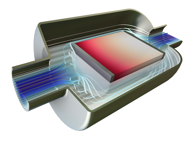 Concentration and velocity of silane gas in the reaction chamber.
Results
The first plot in this section shows the concentration profile of silane in the wafer bundle, which strongly influences the deposition rate and thickness of the deposited silicon layer and is used to estimate the rate of silicon deposition on the wafer bundle. The highest concentration is observed near the inlet and the free flow domain. While one typically wants the concentration to be as even as possible, a high concentration has its own benefit of reducing deposition time. To increase the concentration in the gas diffusing into the wafer bundle, the flow rate of the gas around the wafer can be increased.
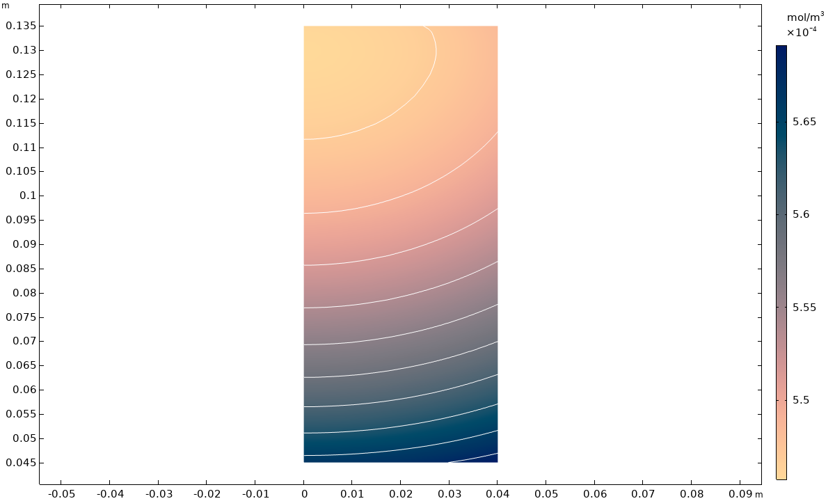 The concentration profile of silicon, where the lines represent isocontours.
The plot below depicts the variation in silicon deposition rate with temperature, pressure, and location in the wafer bundle. Each pair of curves of a particular color indicates the minimum and maximum expected deposition rate when operating at different pressures in the CVD process.
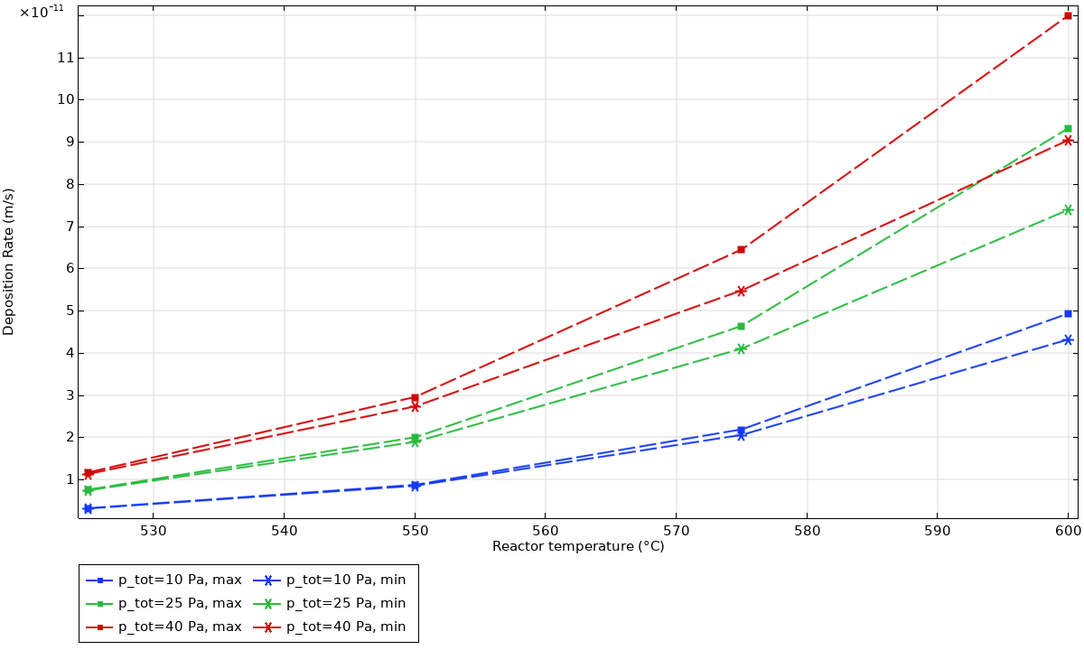 The minimum and maximum expected deposition rates for different values of pressure.
This plot shows that the variation in silicon deposition rate increases with both the operating temperature and the pressure of the reactor. From these results, we can determine that in order to ensure a uniform deposition rate over the wafer bundle, operating at lower pressures and higher temperatures is more suitable due to the higher diffusivity of silane gas.
Next Step
CVD is an important step in the process of manufacturing microchips. The process can be fine-tuned, but it requires a lot of control. The thickness and uniformity of coatings can be controlled by adjusting the temperature, pressure, and deposition time. Additionally, CVD reactors can be expensive, and the equipment and precursor gases can be hazardous. COMSOL Multiphysics® can be used to model the process, gain a better understanding of the various factors that affect CVD, and fine-tune the outcome.
To get hands-on experience with the model presented here, click the button below.


Comments (0)