
Genome editing in somatic cells shows potential for treating a wide variety of genetic diseases. Since the development of CRISPR-Cas9, a powerful genome editing tool, the demand for DNA synthesis technology has been increasing. A startup company based in the U.K. is developing a desktop platform for highly parallel, accurate, and scalable DNA synthesis that will broaden the horizons of synthetic biology.
New Frontiers in DNA Research
DNA synthesis is traditionally done by first chemically building up a string of bases to create a segment of an individual strand, then attaching the strand segments to each other to form the double-stranded DNA. This can be costly and extremely time consuming, limiting the progress of crucial synthetic biology applications. A desktop DNA platform that can synthesize entire gene sequences would change the landscape of DNA synthesis in every lab. Evonetix, a startup based in Cambridge, U.K., is developing a silicon lab-on-chip system to make this goal a reality.
The platform Evonetix is developing includes a silicon chip that contains multiple reaction sites, each of which can synthesize a distinct DNA strand in parallel. The individual sites have a layer of gold on which the biochemical reactions take place. There are also guard regions that thermally isolate the sites from the passive regions in between.
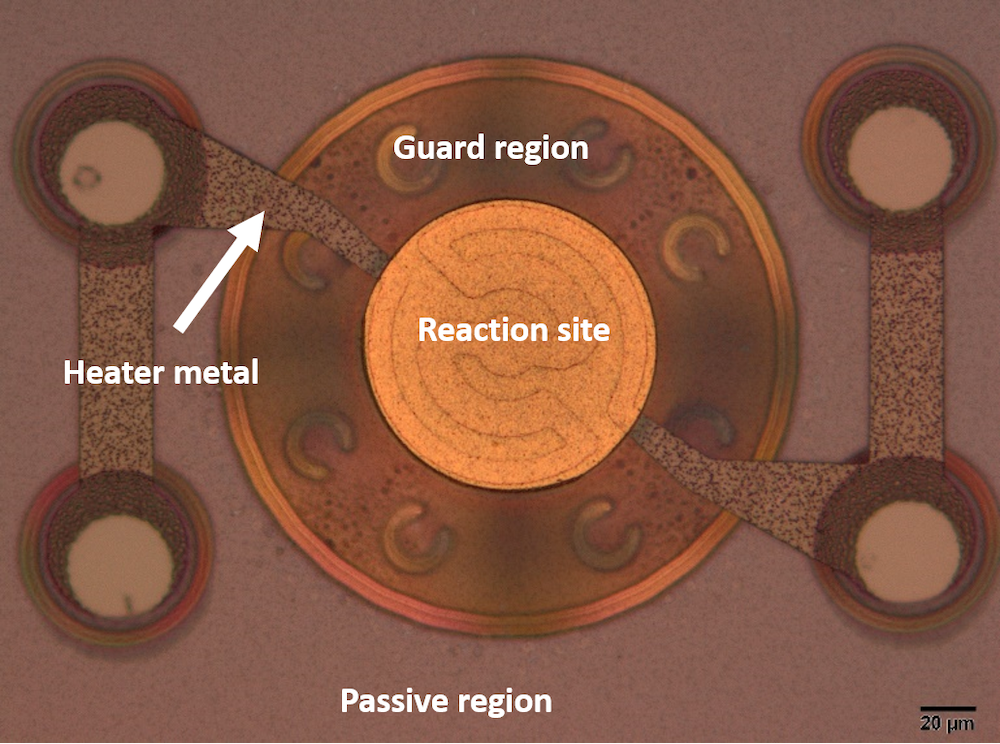
An individual reaction site on the silicon lab-on-a-chip. Image courtesy Evonetix.
Thermal control is one of the most important aspects of the chip. It is used to accelerate and decelerate reactions on individual sites on the chip, effectively switching these on and off like a light switch. Thermal control also enables the temperatures of the fluid volumes at the reaction sites to be controlled both precisely and independently of each other — this control creates “virtual thermal wells”, eliminating the need for physical barriers between reaction sites and allowing the flow of reagents over many thousands of sites simultaneously. This way, when liquid containing chemical reagents flows over the sites, reactions occur (or don’t) depending on the temperature in a highly parallel format.
Another aspect of the chip is its proprietary error detection method, which enhances yield. DNA sequences grown on the reaction sites are automatically purified to remove errors before combining them into longer, high-fidelity gene sequences.
Design Goals
In order for the silicon chip to synthesize DNA as effectively as possible, the Evonetix team had to optimize its geometry and materials. They had three main design goals for the chip:
- Uniform temperature across the reaction site
- High temperature rise per unit power at the reaction site
- Robust temperature profile during fluid flow
Uniform temperature is important because it enables precise control over the reactions. “The chemical reactions are turned on with temperature, and we want to accurately control the rate of reactions,” says Andrew Ferguson, Head of Physics at Evonetix. A high temperature rise per unit power maintains a low overall power requirement for the chip. Lastly, a robust temperature profile on the chip ensures that the reactions can take place under fluid flow conditions.
Modeling a Silicon MEMS Chip in COMSOL Multiphysics®
The Evonetix team uses the COMSOL Multiphysics® software to simulate DNA synthesis on their silicon chip design. “I like the user interface of COMSOL Multiphysics; we can concentrate on the physics while being certain that the numerical implementation of the equations is well taken care of,” says Vijay Narayan, senior engineer at Evonetix. They set up the model with realistic material parameters using built-in materials in COMSOL Multiphysics, as well as external material data from literature.
The team used COMSOL Multiphysics to first find an optimal geometry for a single unit of the chip, including the reaction site and heater, that meets the three design requirements listed above. The ECAD Import Module enabled them to easily import their designs from GDS, a CAD file format, into COMSOL Multiphysics. “The design of the system, especially the heater, can be very precise, and has very strict design rules,” says Narayan. “The ECAD Import Module provides an extra degree of flexibility.” This functionality also enables the group to bring designs directly to the manufacturer when they reach the prototyping stage.
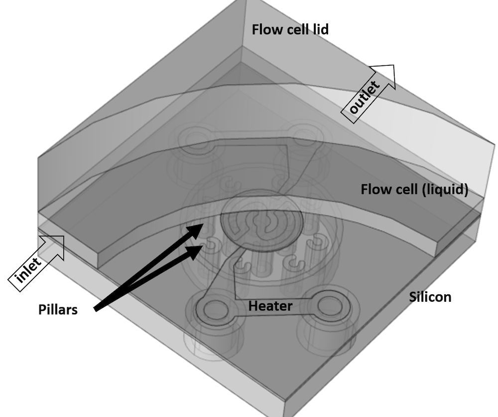
The simulation model including one reaction site. Image courtesy Evonetix.
To analyze the steady-state and transient thermal responses of the system, the team used the Heat Transfer Module. They evaluated the temperature control capabilities of the system by passing a current through the heater using the Electromagnetic Heating interface. To extend the thermal analysis, the team included fluid flow by adding the Laminar Flow interface and Nonisothermal Flow multiphysics coupling.
Comparing the Model to Experiment
After using simulation to predict the optimal geometry and materials for the silicon chip, Evonetix was ready to move on to the prototyping stage. They used the prototype chips to run electronic tests, then compared the results to the COMSOL Multiphysics simulations.
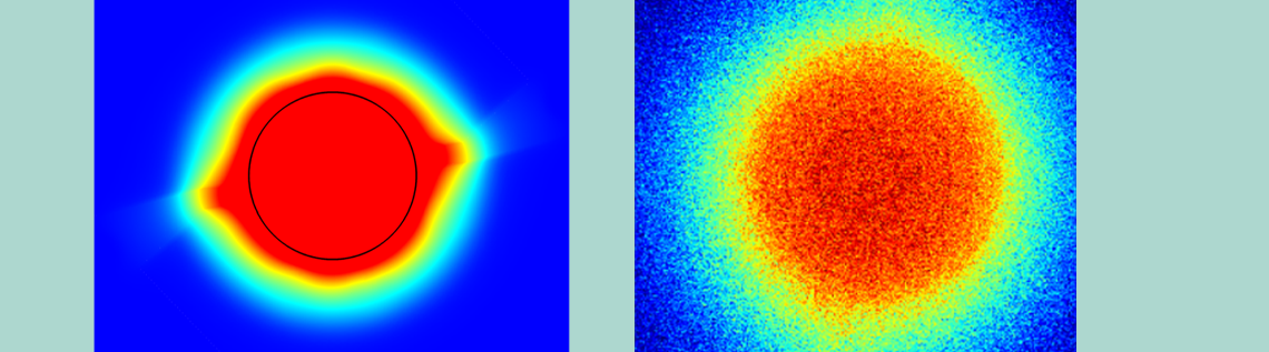
The simulation results for temperature distribution on the reaction site surface showed excellent temperature uniformity (design requirement #1, as listed above) with only small deviations around the heater leads. To confirm these results, the team turned to epifluorescence microscopy, using a molecule whose fluorescence depends on temperature. This allowed them to see the actual temperature distribution in the fluid above the reaction sites, confirming the model’s predictions of a sharply-defined thermal well and a uniform temperature across the reaction site.
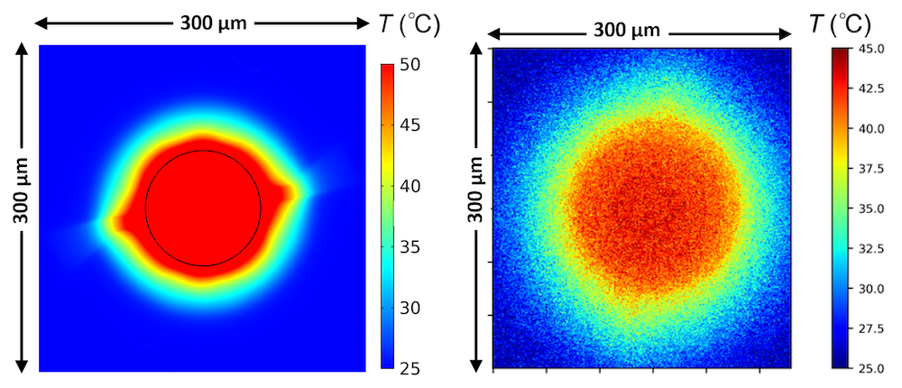
Thermal analysis of the reaction site (left) compared to epifluorescence microscopy results (right). Images courtesy Evonetix.
The Physics team also looked at the temperature profiles along the reaction site for different currents, determining the temperature rise per unit power (design requirement #2). In fact, the temperature outside of the site’s guard region is only negligibly affected by the heater’s heat dissipation. This shows that the crosstalk between sites is negligible, which was also verified by experiments.
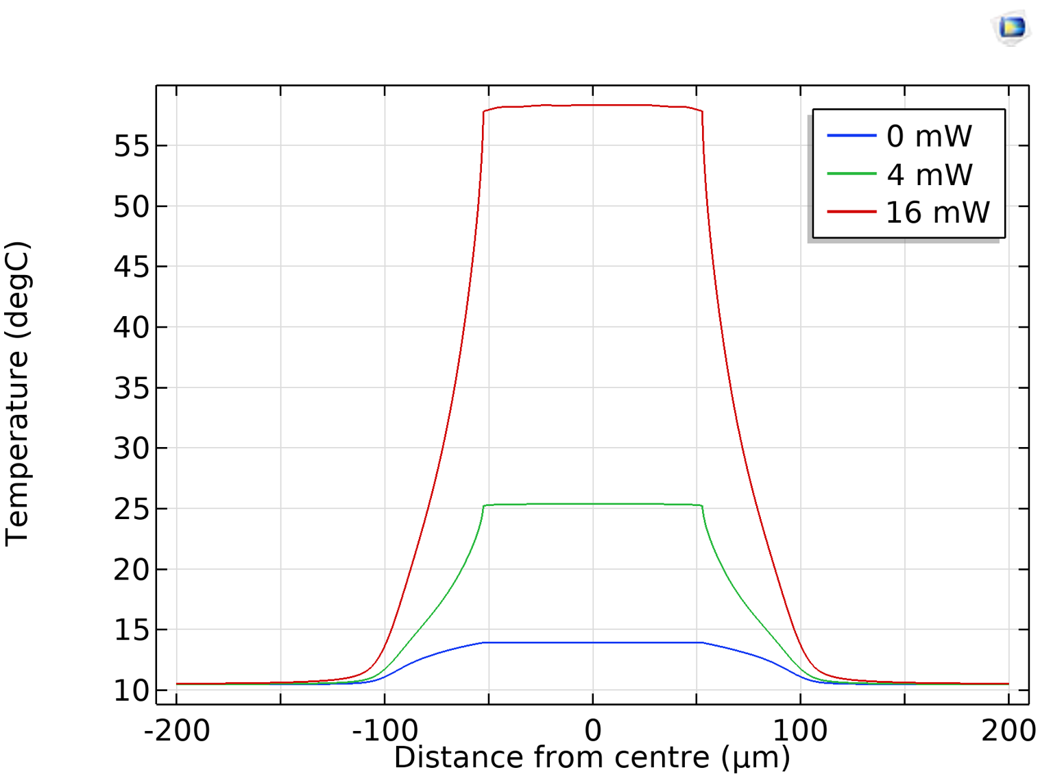
Temperature profiles for the reaction sites at different voltages. Image courtesy Evonetix.
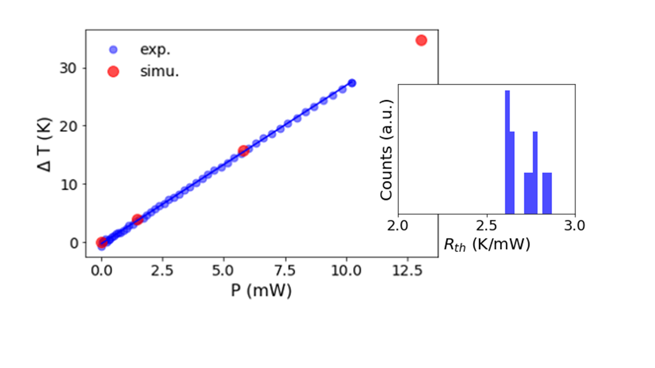
Comparison of the temperature rise in the simulation and experiments. An experimental histogram of the slope of temperature rise vs. power (right inset) is tightly centered on the simulated value of 2.7 K/mW. Image courtesy Evonetix.
Finally, the Physics team wanted to see how the fluid flow affects the reaction sites. Both the simulation results and experiments suggest that for liquid velocities up to 1 mm/s (the maximum velocity they plan to use for synthesis), the thermal well profile doesn’t change.
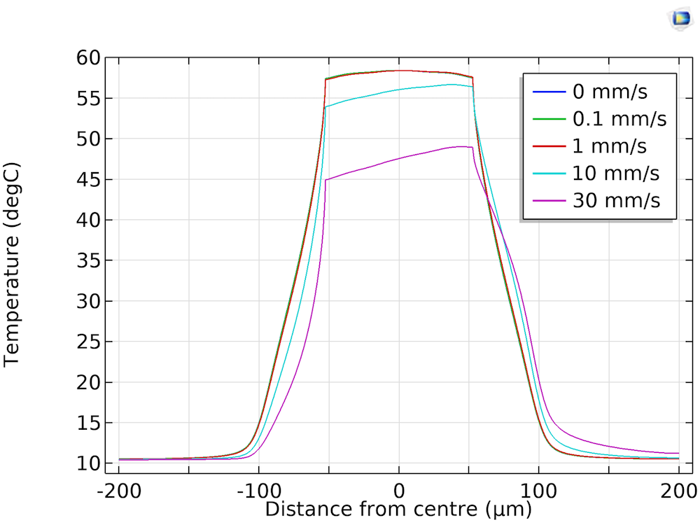
Temperature profile of the reaction site when subject to increasing flow rates. Image courtesy Evonetix.
The Evonetix team used COMSOL Multiphysics to help optimize the properties of their Si lab-on-a-chip system, which was then prototyped and experimentally verified. Overall, the chip performance matched very well between experiment and simulation. Simulation also helped them work within the manufacturing constraints, including requirements for materials and cost.
Future Plans
Evonetix plans to significantly expand the scope of simulations: they first propose to incorporate chemical reactions into the existing model to simulate the DNA synthesis process. This would then be further progressed to include multiple reaction sites, fluid inlet/outlets, and external heat sources/sinks, ultimately creating a digital model of the end product. The results will assist in optimizing individual components, including the chip, reagent influxes, and peripheral hardware; and ultimately toward delivering an optimized system.
Further Reading
- Learn more about Evonetix’s research in their paper presented at the COMSOL Conference 2019 Cambridge: “Towards high throughput DNA synthesis in a silicon-based MEMS ‘virtual thermal well’ array“
- Read about another way simulation is used for DNA sequencing on the COMSOL Blog
- Learn more about the CRISPR-cas9 project via Your Genome


Comments (1)
Ameya Abhay Kale
May 26, 2020Hi!
Great post! I wanted to ask if a model of the same tutorial will be released on the blog? It would be really helpful if I could try implementing it myself.
Thank you, and keep up the great content!
Ameya