In a previous blog post, we briefly introduced the density-gradient theory (Ref. 1), which accounts for the effect of quantum confinement in the conventional drift-diffusion formulation without requiring excessive additional computational costs. Therefore, this theory can afford much speedier engineering investigations than other, more sophisticated quantum mechanical methods. Here, we continue with three examples to showcase the advantage of this modeling approach for semiconductor device physics simulation.
Example 1: Si Inversion Layer
The metal-oxide-silicon (MOS) structure is the fundamental building block for many silicon planar devices. The inversion layer under the oxide-silicon interface has been studied extensively using various techniques. In this first example, a silicon inversion layer based on Ref. 2 is simulated using the conventional drift-diffusion formulation, the density-gradient theory, and the fully quantum mechanical Schrödinger–Poisson equation. The thickness of the gate oxide is 3.1 nm and the doping concentration is 3.8e16 1/cm3. The density-gradient effective mass is 1/3 of the electron mass. The temperature is 300 K and Fermi-Dirac statistics are used.
As shown in the graphs below, the resulting electron concentration distribution from the drift diffusion (labeled “DD”) clearly lacks the effect of quantum confinement, and the one from the density gradient (labeled “DG”) is very close to the one from the Schrödinger–Poisson equation (labeled “SP”).
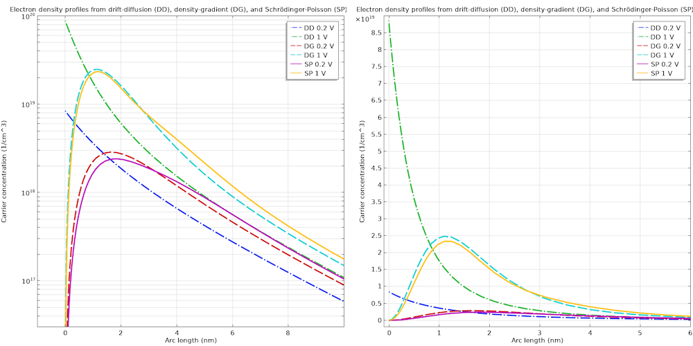
Electron density profiles from the conventional drift-diffusion formulation (DD), density-gradient theory (DG), and Schrödinger–Poisson equation (SP). Left: log scale, right: linear scale.
While the density-gradient result does not match exactly with the result from the fully quantum mechanical treatment, it offers an enormous improvement over the conventional drift-diffusion formulation. In addition, it takes a lot less computational resources than the Schrödinger–Poisson equation. In this simple 1D model, the computation time for the density gradient is 6 seconds and the one for the Schrödinger–Poisson equation is 253 seconds. The difference will grow much larger for more complex models in higher dimensions.
Example 2: Si Nanowire MOSFET
This 3D model of a silicon nanowire MOSFET is based on Ref. 3. The channel of the simulated structure is formed by a rectangular silicon nanowire with a 3.2-nm square cross section surrounded by an oxide layer of thickness 0.8 nm. The length of this channel is 4 nm, and the temperature is kept at 300 K. Maxwell–Boltzmann statistics are consistently used in the reference paper as well.
The density-gradient effective mass is anisotropic in this model. This is done by selecting the Diagonal option under the section Material Properties, Density-Gradient in the Settings window for the Semiconductor Material Model domain condition, as shown in the screenshot below.
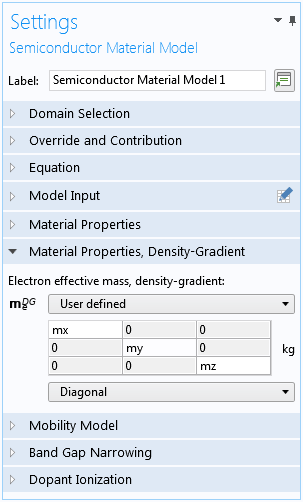
Settings for an anisotropic effective mass matrix.
The oxide layer is modeled explicitly using the Charge Conservation domain condition. The quantum confinement effect at the silicon-oxide interface is incorporated by selecting the Potential barrier option for the Insulator Interface boundary condition, as shown in the screenshot below. This option implements the boundary condition described in Ref. 4 and discussed briefly in the previous post.
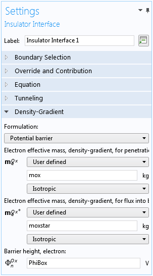
Settings for adding quantum confinement at semiconductor–insulator interfaces.
The I-V curves and electron density profiles shown in the following figures all agree well with the corresponding figures in Ref. 3.
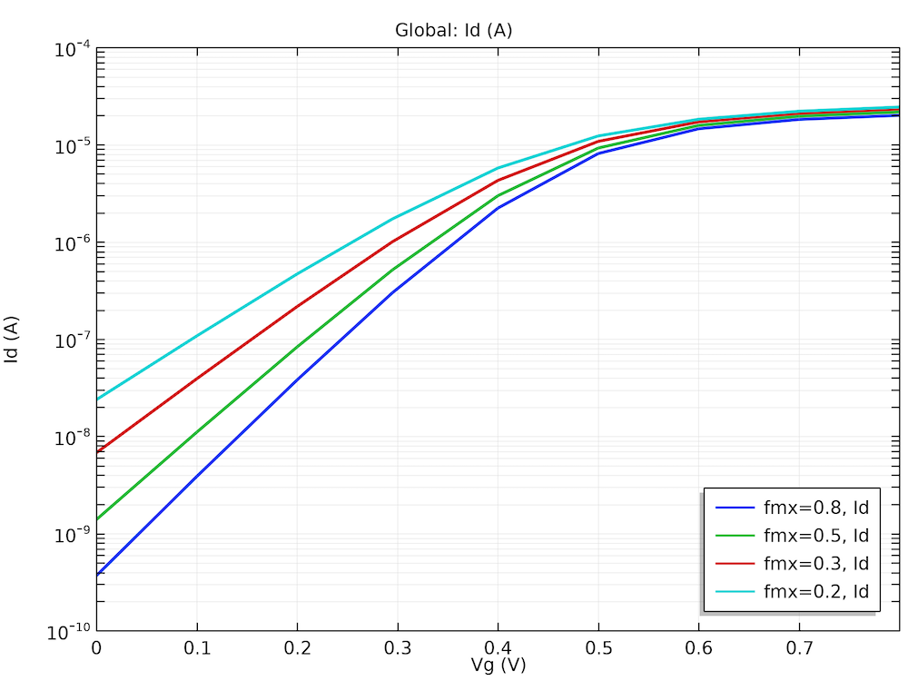
I-V curves for a set of density-gradient longitudinal effective masses.
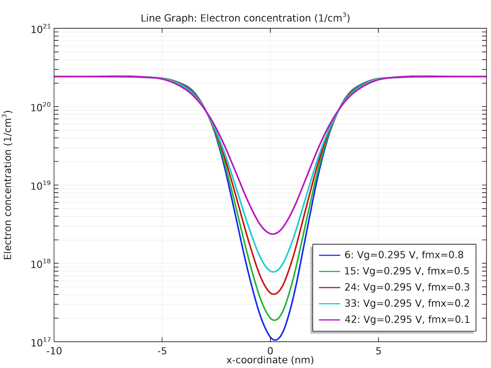
Longitudinal electron concentration profiles for a set of density-gradient longitudinal effective masses.
![]()
Transverse electron concentration profiles for a set of density-gradient longitudinal effective masses.
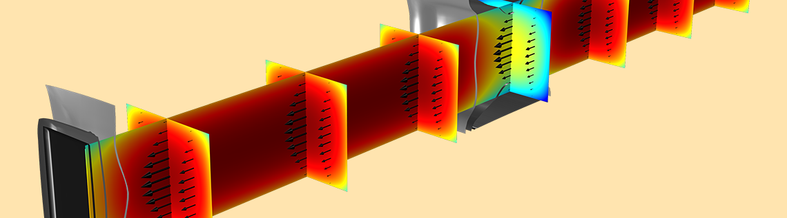
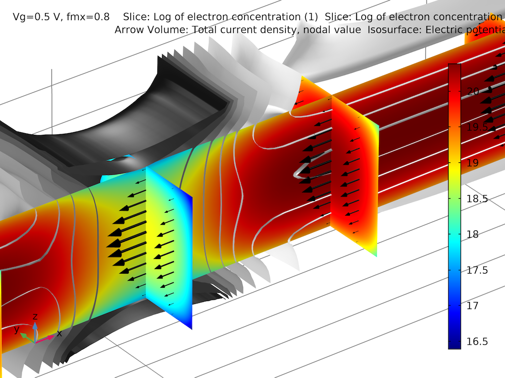
In the last graph above, the effect of quantum confinement at the oxide–silicon interface is evident. The graph below provides a snapshot of the 3D distribution of the electron density (color slices), the current density (black arrows), and the electric potential (grayscale isosurfaces).
Example 3: InSb p-Channel FET
This model analyzes the DC characteristics of an InSb FET with a nanometer scale channel based on Ref. 5. The channel of the simulated structure is formed by a 5-nm thick InSb quantum well layer built on top of an AlInSb barrier material. A 10-nm thick barrier layer is then added on top of the quantum well layer, followed by the p+ caps for the source and drain contacts. The temperature is 300 K and Fermi–Dirac statistics are used.
The quantum confinement effect for the quantum well layer is automatically accounted for with the default Continuous quasi-Fermi levels option for the Continuity/Heterojunction boundary condition, active at the well-barrier interfaces. In addition, the quantum confinement effect for the top barrier layer boundary (the top barrier–vacuum interface) is added by selecting the Potential barrier option for the Insulation boundary condition, in a similar fashion as the previous example. The density-gradient effective mass is anisotropic and is set up in the same way as the previous example.
A field-dependent mobility model is employed by the reference paper. Given the simple geometry, it is sufficient to use the x component of the electric field for the mobility model. However, we opt for the more general procedure, applicable to any arbitrary geometry. A Caughey-Thomas Mobility Model (E) subnode is added to the Semiconductor Material Model domain condition to provide the parallel component of the electric field, which is used by the mobility model. The solver sequence is adjusted to achieve convergence for the resulting highly coupled system by delaying the update of the parallel component of the electric field with the Previous Solution node, as shown in the screenshot below.

Use the Previous Solution node in the solver sequence to delay the update of the parallel component of the electric field to achieve convergence for the general case of the arbitrary geometry.
The I-V curve and hole density profile shown in the following graphs match reasonably well with the figures in Ref. 5.
I-V curve of the InSb FET model.
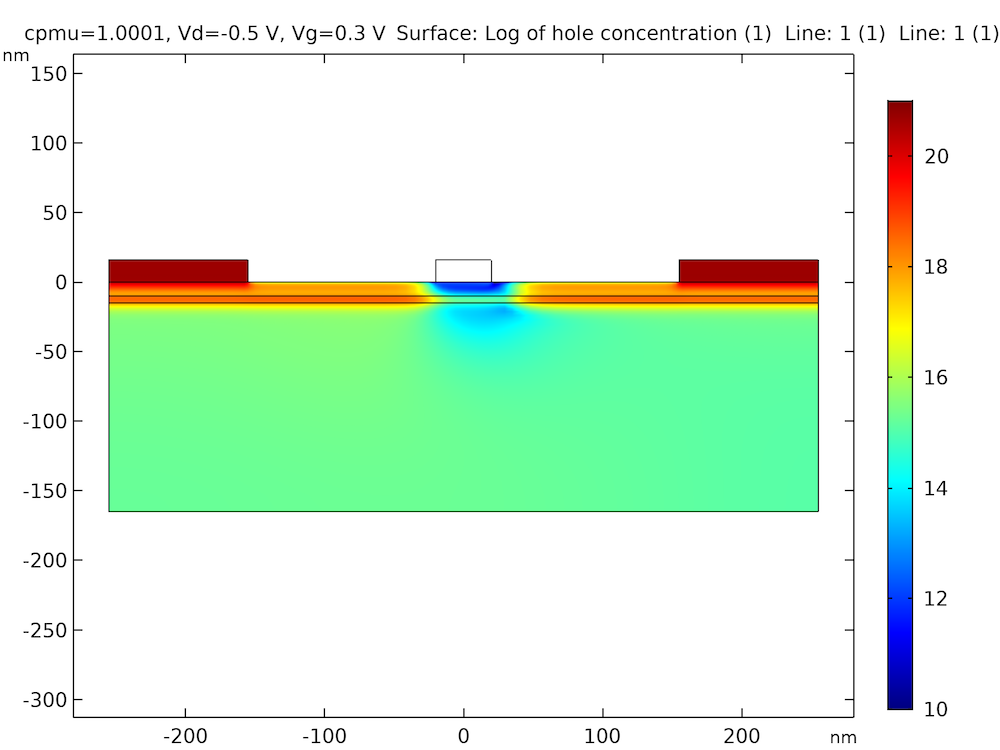
Hole concentration profile showing the quantum confinement effect.
The figure below compares a line cut of the hole density profile at x = -100 nm (blue curve) with an approximate drift-diffusion profile (red dotted curve), to show qualitatively the effect of quantum confinement both in the quantum well layer and at the top barrier–vacuum interface (y = 0 nm). The valence band edge (“Ev”) and the quasi-Fermi level for the holes (“Efp”) are also plotted. Note that this comparison is only qualitative, since the model is not re-solved using the conventional drift-diffusion formulation. As such, only the shape of the approximate drift-diffusion profile is representative of the result, if the model was to be re-solved and the absolute magnitude was not. Nevertheless, the qualitative difference between the treatments with and without quantum confinement is well characterized by the difference in the shape of the hole concentration profiles: The lack of carrier pileup at the heterojunctions and the repulsion of carriers from the top barrier–vacuum interface are both clearly indicative of quantum confinement effects.
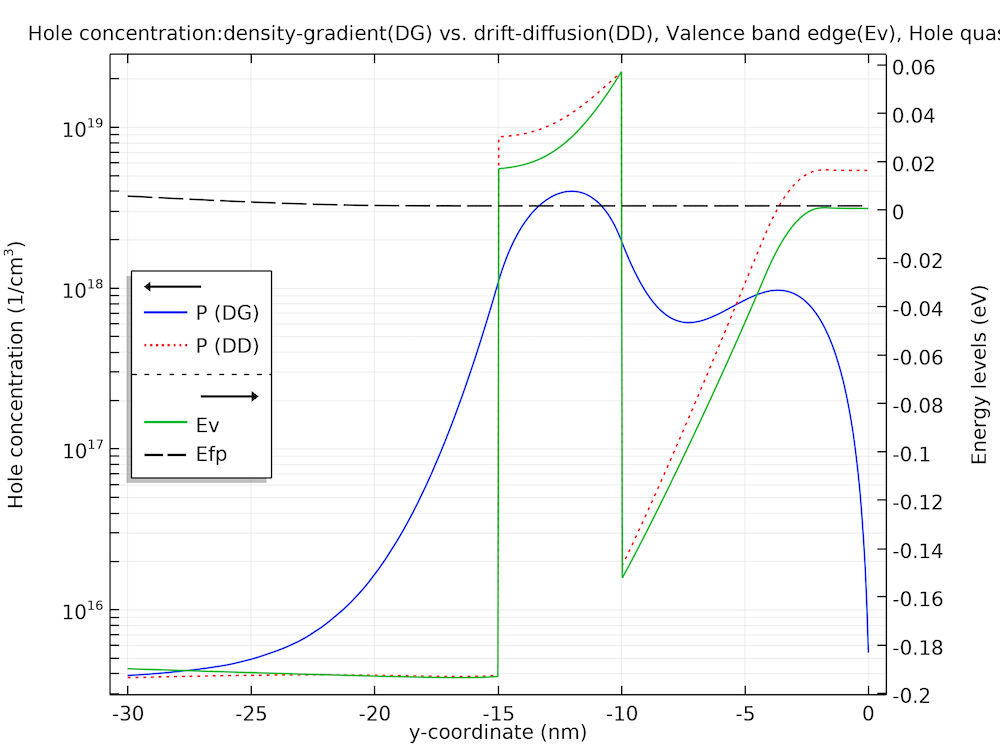
Line cut plot to elucidate the quantum confinement effect.
Final Remarks on Modeling Semiconductor Devices
As the physical sizes of transistors continue to shrink, the effect of quantum confinement can no longer be ignored. To include this effect in device physics simulations, we have introduced the computationally efficient density-gradient theory and some modeling examples in this two-part blog series.
Next Steps
Download the tutorial models featured in this blog post:
- Density-Gradient and Schrödinger-Poisson Results for a Silicon Inversion Layer
- 3D Density-Gradient Simulation of a Nanowire MOSFET
- Density-Gradient Analysis of an InSb p-Channel FET
To try out the density-gradient formulation yourself, click the button below to contact us for an evaluation license.


Comments (0)