
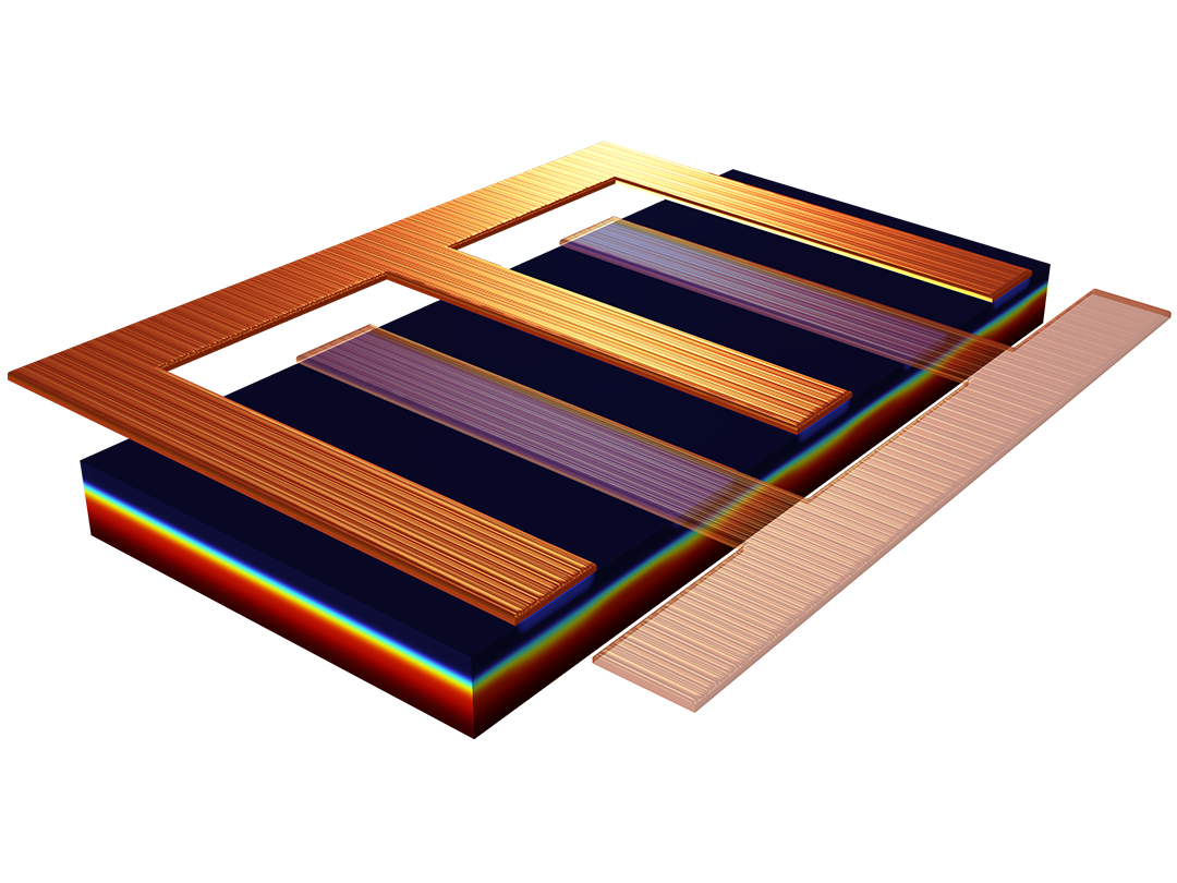
3D Bipolar Transistors
Compute the current–voltage response of a bipolar transistor and simulate the device's operation as an analog current amplifier.
Simulate Semiconductor and Optoelectronic Devices
The Semiconductor Module provides dedicated features for the analysis of semiconductor device operation at the fundamental physics level. A range of common device types can be simulated with the Semiconductor Module, including bipolar transistors, metal–semiconductor field-effect transistors (MESFETs), metal–oxide–semiconductor field-effect transistors (MOSFETs), insulated-gate bipolar transistors (IGBTs), Schottky diodes, p–n junctions, solar cells, and more.
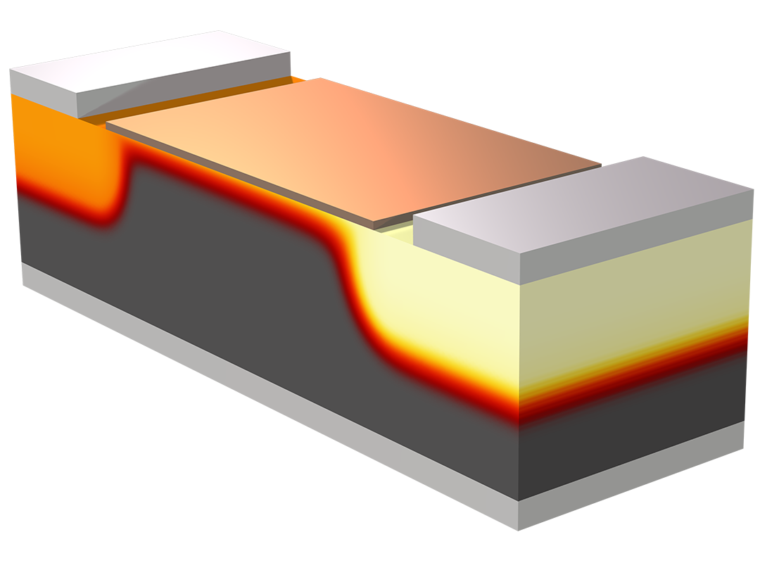
The module includes features designed to model interactions of electromagnetic waves and semiconductor materials. Typical modeling devices are photodiodes, LEDs, and laser diodes. In addition, the module makes it possible to employ user-defined equations and expressions in the modeling process.
The Semiconductor Module also has the flexibility to be combined with any other COMSOL Multiphysics® add-on product.
Contact COMSOL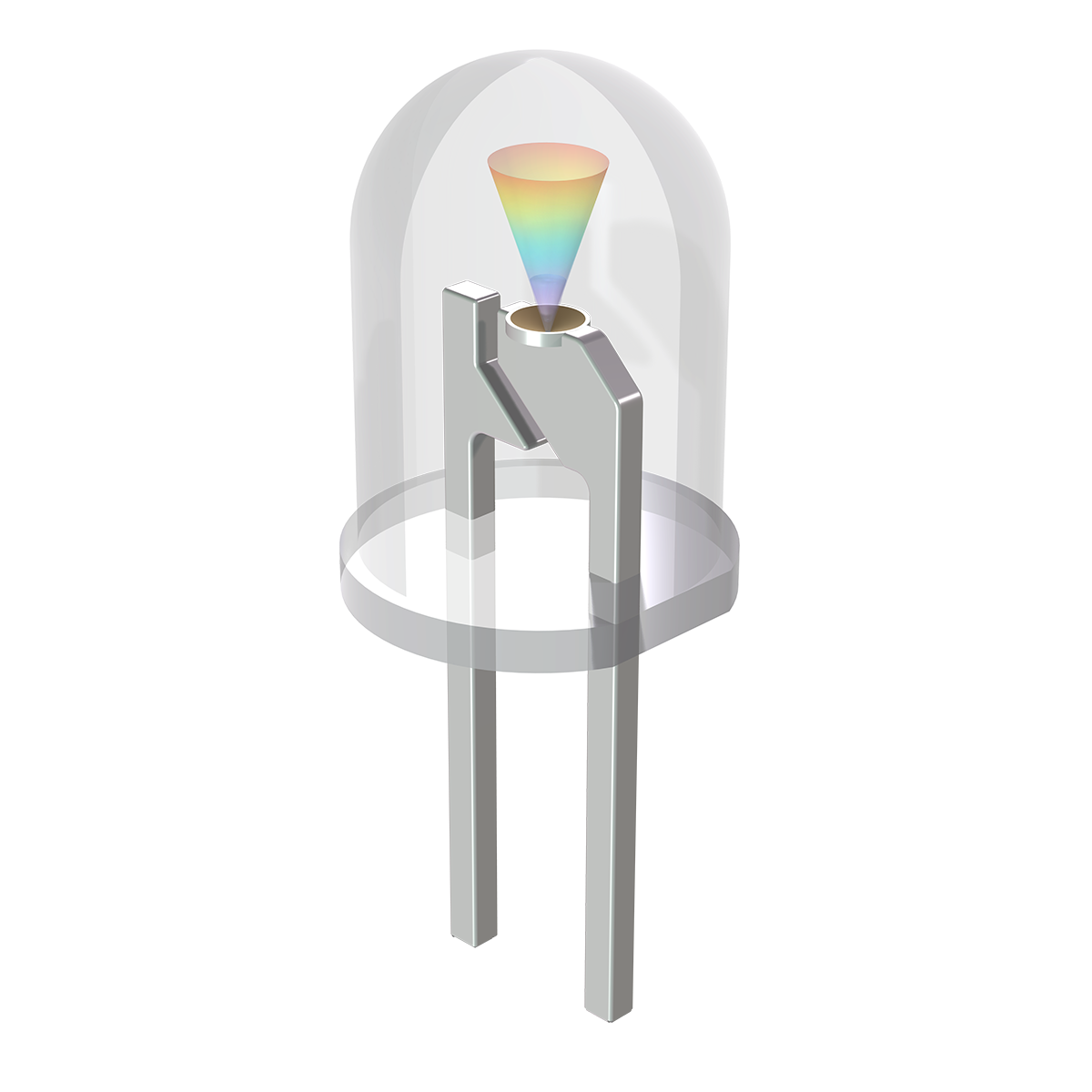
Analyze various kinds of transistors, sensors, photonic devices, quantum systems, and basic semiconductor building blocks.
Compute the current–voltage response of a bipolar transistor and simulate the device's operation as an analog current amplifier.
Calculate the DC characteristics of a metal–oxide–semiconductor (MOS) transistor.

Compute user-defined generation (deformed) and Shockley–Read–Hall recombination rates of solar cells.
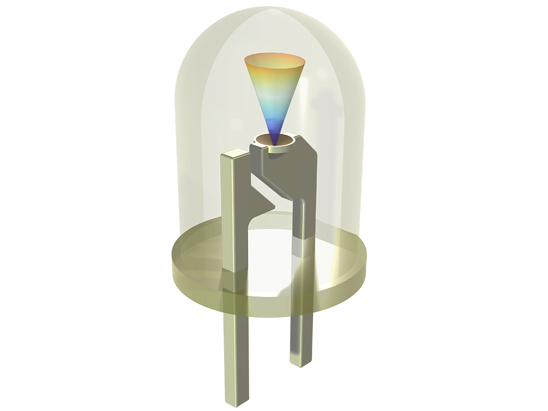
Simulate an LED that emits infrared light.
Couple a semiconductor model and an electrolyte model to simulate an ion-sensitive field-effect transistor (ISFET) pH sensor.
Model a trench-gate IGBT, arranging the alternating emitters along the direction of extrusion as in a real device.
Analyze the DC characteristics of an InSb p-Channel FET, using the density-gradient formulation to add quantum confinement.
Solve the Gross–Pitaevskii equation for the vortex lattice formation in a rotating Bose–Einstein condensate.
Explore the features and functionality of the Semiconductor Module in more detail below.
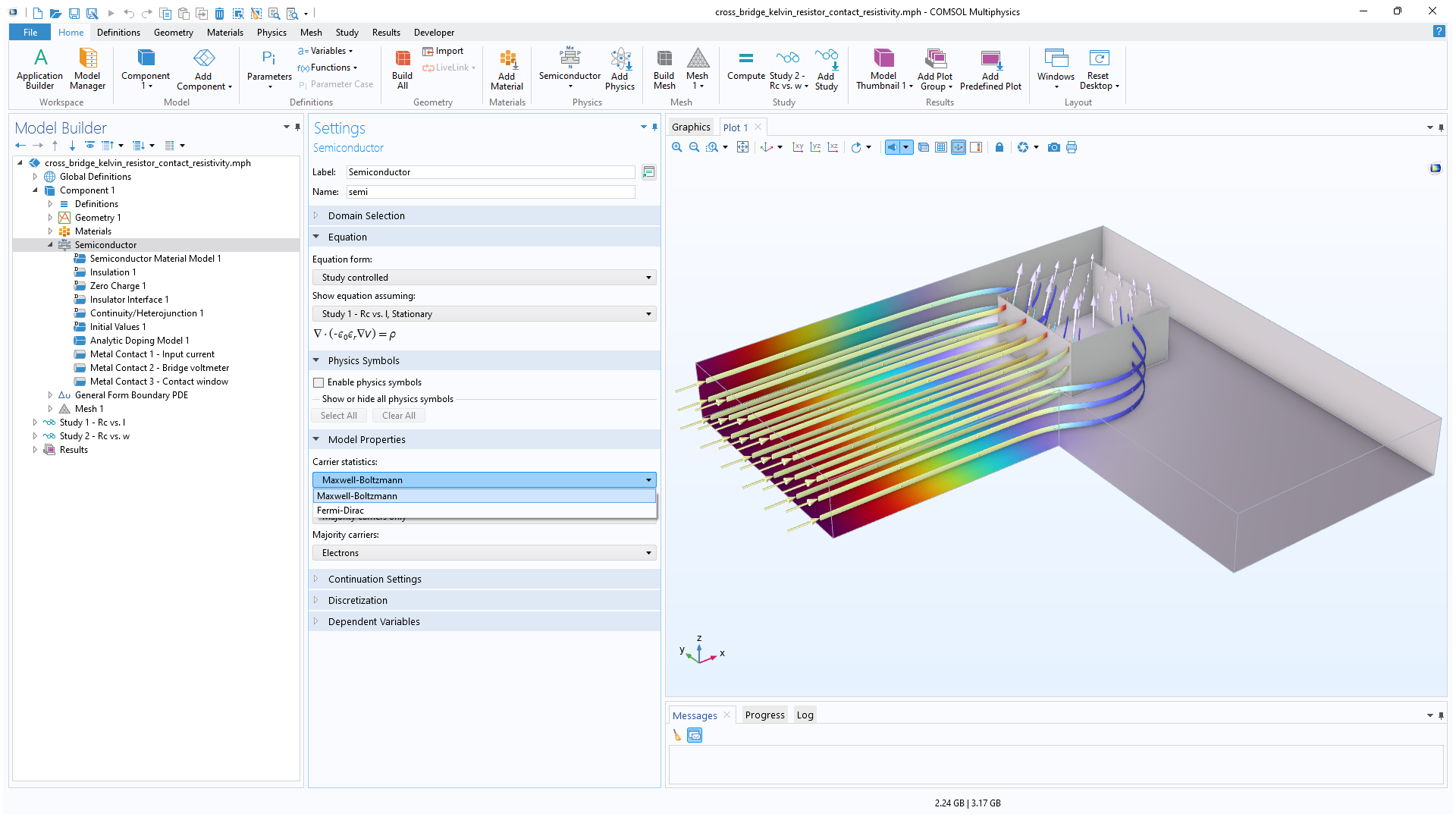
The cornerstone of the Semiconductor Module is the Semiconductor interface, which solves the combined drift–diffusion and Poisson’s equations. This interface allows for modeling both insulating and semiconducting domains in a semiconductor device. One application of the drift–diffusion formulation is to simulate the fundamental physics of a device using Fermi–Dirac or Maxwell–Boltzmann statistics.
The available analysis types for drift–diffusion equations include thermal equilibrium, steady-state, transient response, and small-signal analysis.
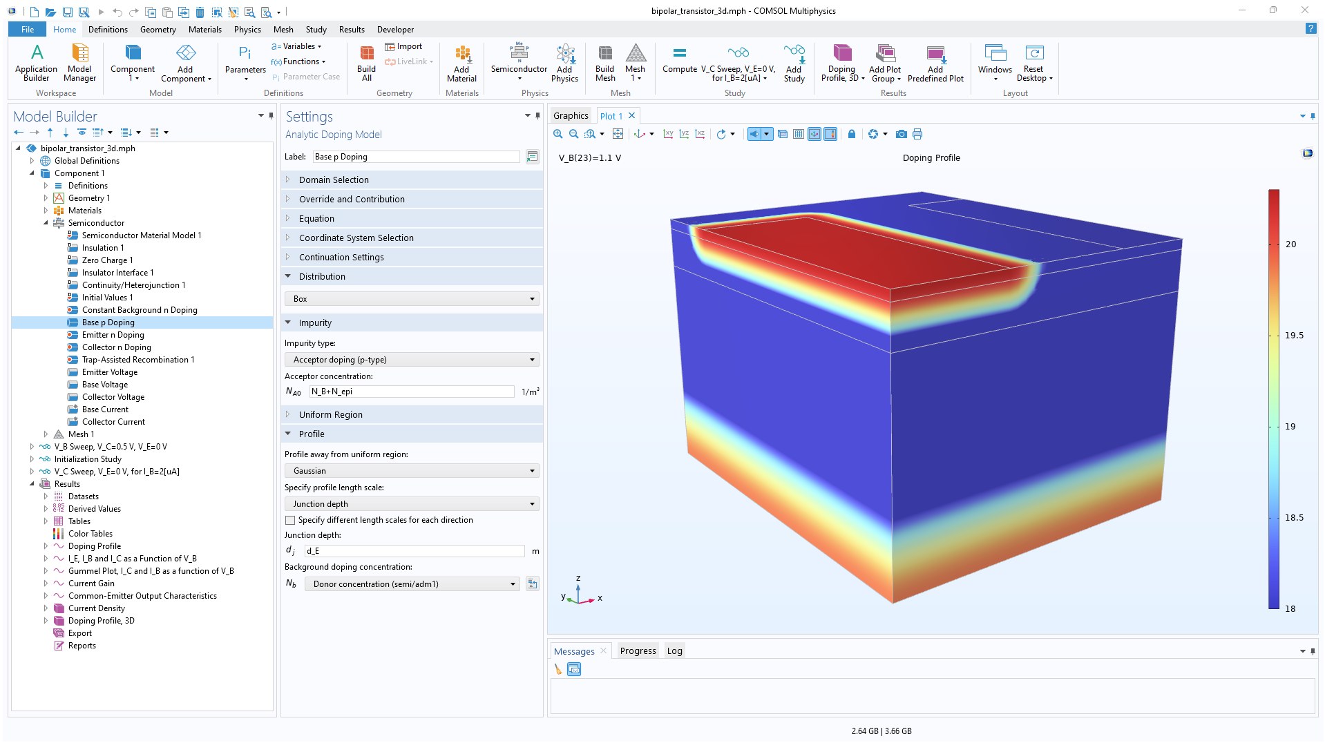
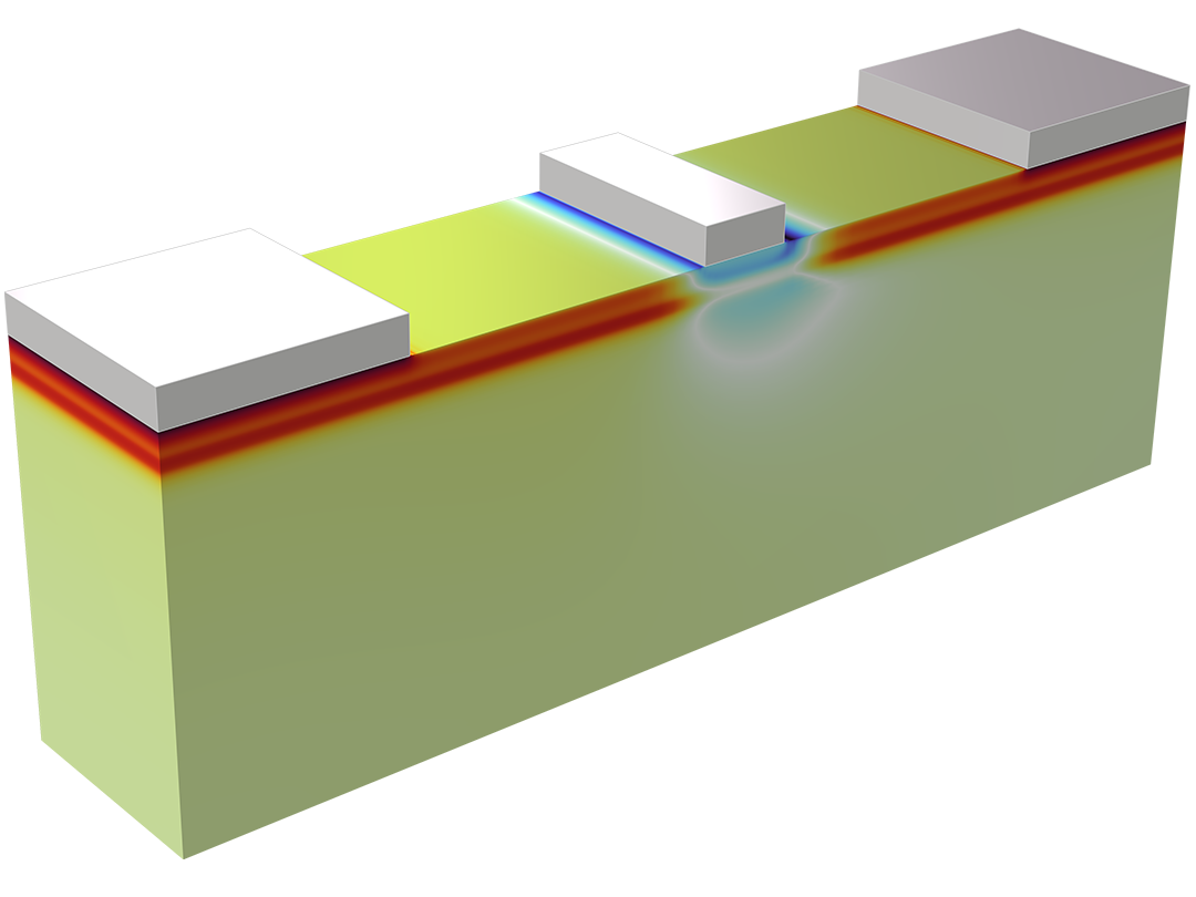
Specifying the doping distribution of a material is critical for the modeling of semiconductor devices. The Semiconductor Module includes a range of features that enable virtually any doping profile to be realized. Advanced options include incomplete ionization and, for high doping levels, band gap narrowing.
Built-in options for doping profiles include Linear, Gaussian, and Error function. User-defined doping profiles can be specified by typing a mathematical expression or by using the output from another simulation as a basis for the doping profile.
In addition, it is straightforward to define doping profiles based on imported lookup tables. This strategy is useful when the required distribution cannot be defined analytically, for example, if the doping profile is output from an external simulation.
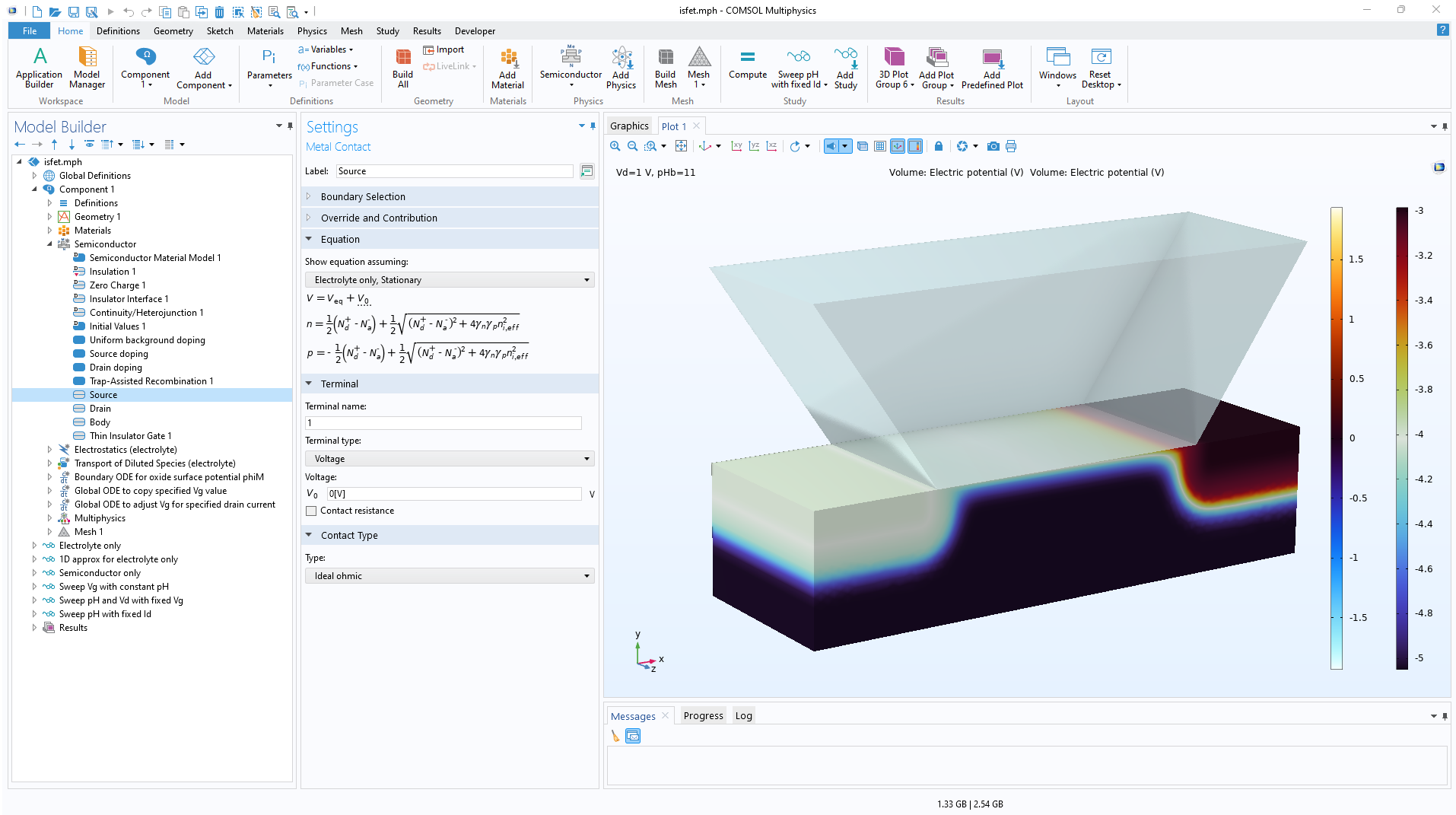
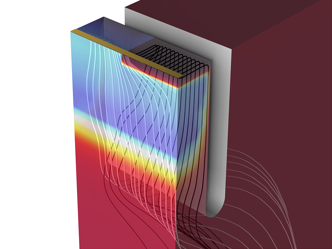
A dedicated Metal Contact boundary feature can be used for modeling metal–semiconductor contacts. This terminal type supports voltage, current, power, and connection to an external circuit.
An ideal Schottky contact type is available for modeling a simple rectifying metal–semiconductor junction where the current–voltage characteristics depend on the potential barrier formed at the junction. To incorporate surface recombination effects and surface charge densities from surface traps in this model, Trap-Assisted Surface Recombination boundary conditions can be added to the same boundary selection as the metal contact condition.
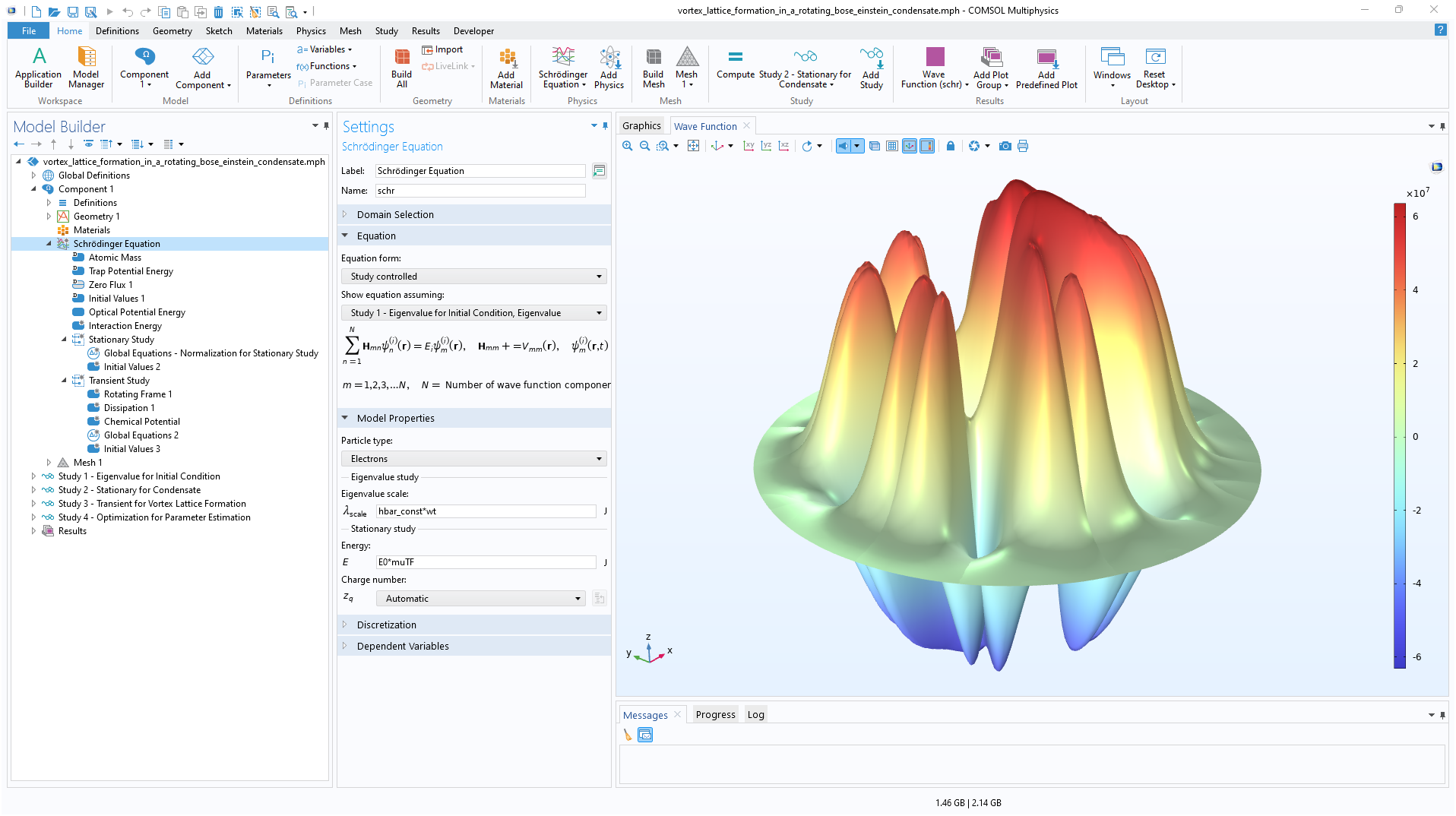
The Schrödinger Equation interface solves the Schrödinger equation for a single particle in an external potential. This interface is useful for general quantum mechanical problems and quantum-confined systems, such as quantum wells, wires, and dots (with the envelope function approximation).
Appropriate boundary conditions and study types are implemented for the user to easily set up models to compute relevant quantities in various situations, such as the eigenenergies of bound states, the decay rates of quasi bound states, the transmission and reflection coefficients, the resonant tunneling condition, and the effective band gap of a superlattice structure.

An Optical Transitions feature is available for modeling optical absorption and both stimulated and spontaneous emission within a semiconductor. Stimulated emission or absorption occurs when a transition takes place between two quantum states in the presence of an oscillating electric field, typically produced by a propagating electromagnetic wave. Spontaneous emission occurs when transitions from a high-energy to a lower-energy quantum state occur.
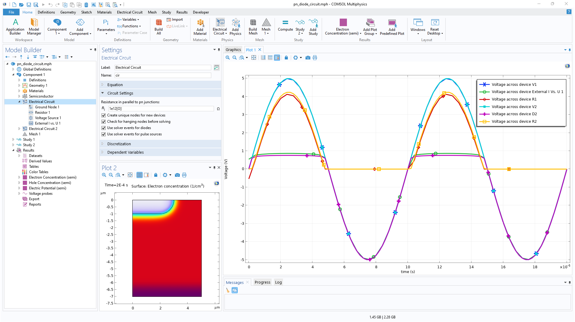
The Electrical Circuit interface is used for creating lumped systems to model currents and voltages in circuits. This functionality is beneficial when modeling typical voltage and current sources, resistors, capacitors, inductors, and other semiconductor devices. Electrical circuit models can also connect to distributed field models in 2D and 3D. Additionally, circuit topologies can be exported and imported in the SPICE netlist format. Electrical circuits can be combined with physics models of semiconductor devices to simulate realistic loads, for example.
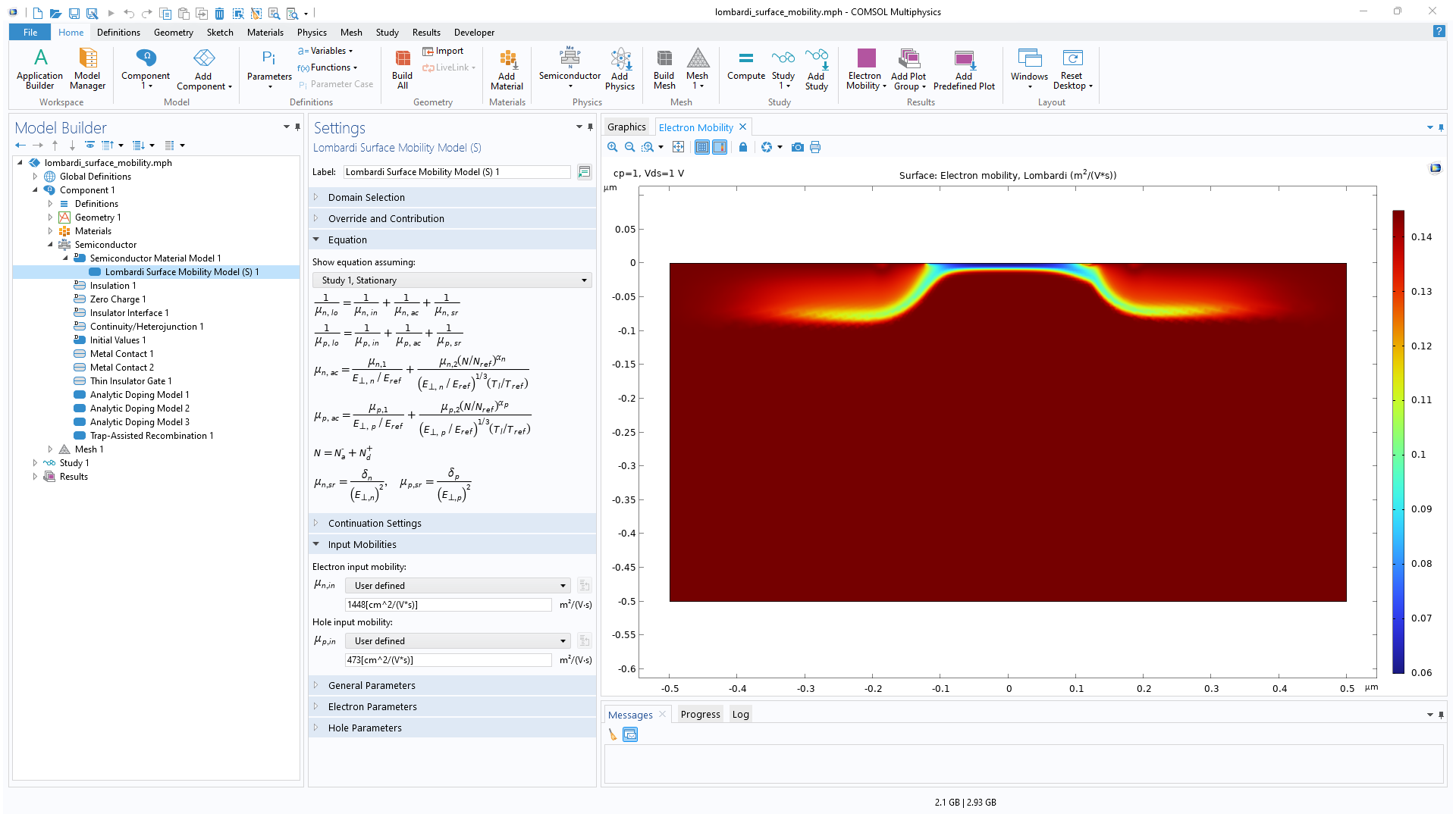
Realistic models for carrier mobility are important when simulating semiconductor devices with a drift–diffusion approach. In these cases, the mobility is limited by a scattering of the carriers within the material. The Semiconductor Module includes several predefined mobility models as well as the option for users to define their own mobility models.
The predefined mobility models include options for phonon, impurity, and carrier–carrier scatterings, high-field velocity saturation, and surface scattering.
User-defined mobility models can be readily specified by typing appropriate expressions into the user-defined feature; scripting or coding is not required. These user-defined mobility models can be combined arbitrarily with the predefined mobility models built into the software.
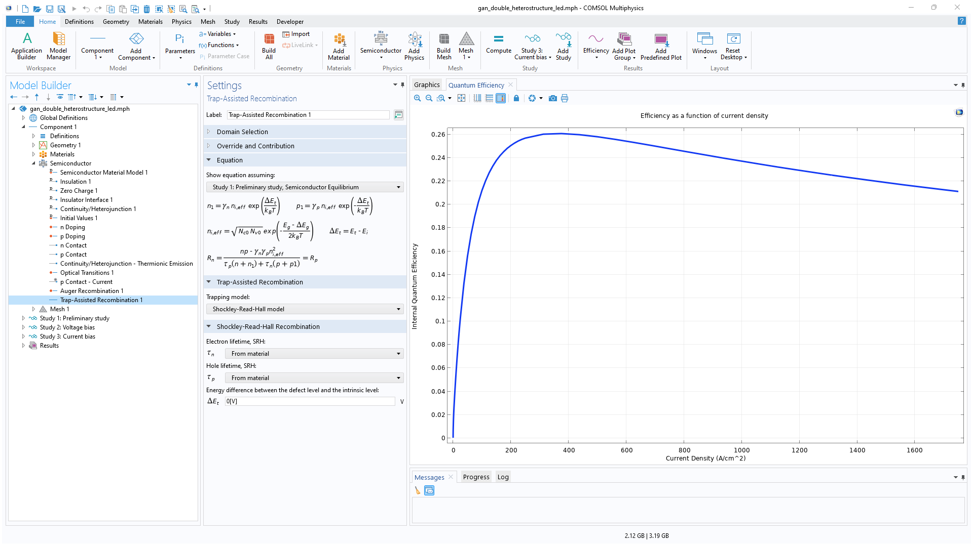
Generation and recombination processes such as Auger recombination, direct recombination, impact ionization generation, and trap-assisted recombination can be included in models using the Semiconductor interface. User-defined recombination and generation features are available to manually set the rates of these processes.
The Trap-Assisted Recombination model is used for setting the electron and hole recombination rates in indirect-band-gap semiconductors. By default, steady-state recombination is modeled using the Shockley–Read–Hall trapping model, which considers states located at the midgap. An Explicit trap distribution model can also be used for specifying discrete traps or continuous density of trap states at energies within the band gap.

The Semiconductor interface includes a feature for modeling a thin insulating material (oxide) between a semiconductor and a metal. This feature also supports small-signal analysis, which is useful for computing I–V curves.
For modeling a general insulator, a charge conservation domain feature can be added to the Semiconductor interface in a way that is similar to how the feature is added when modeling with the general interface for Electrostatics. For insulating domains, several boundary conditions can be modeled, including:
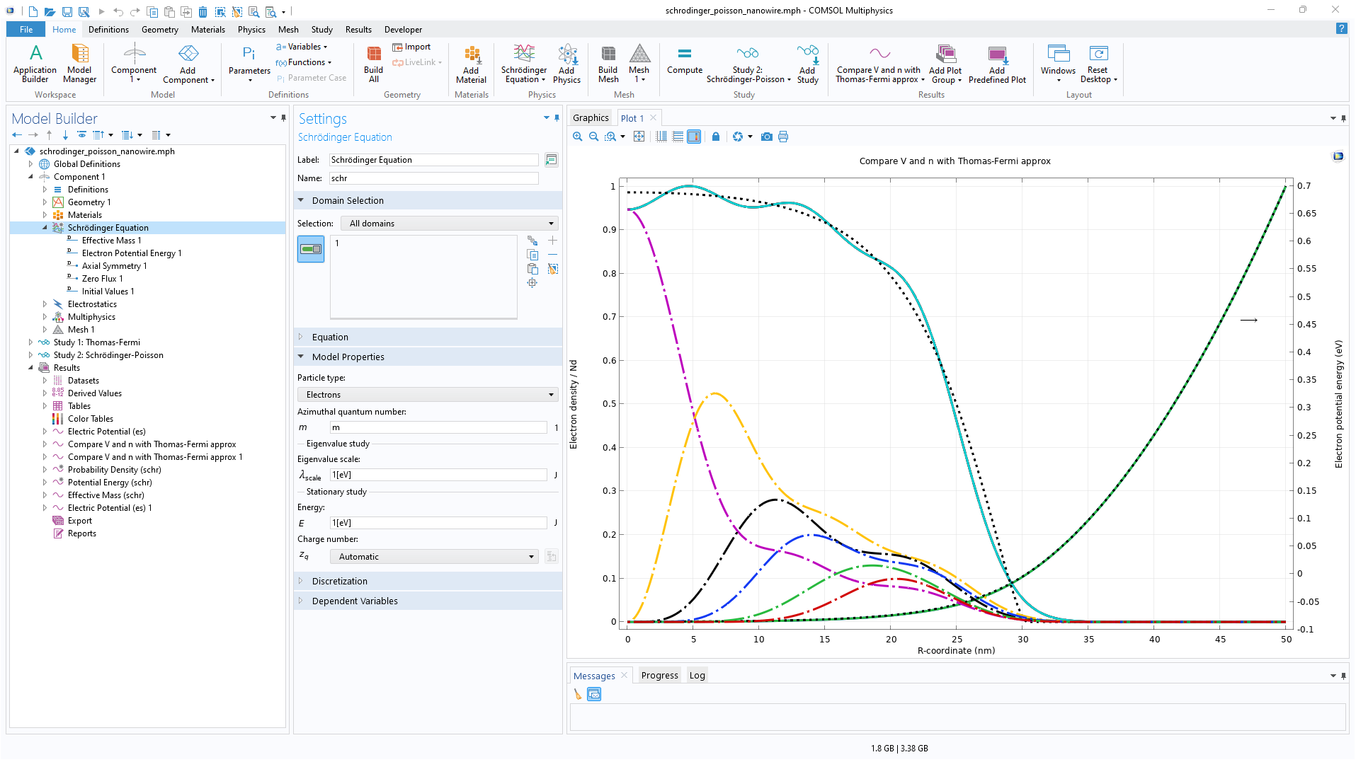
The Schrödinger–Poisson Equation multiphysics interface combines the Schrödinger Equation interface and Electrostatics interface to model charge carriers in quantum-confined systems. This interface can be used for modeling quantum-confined devices such as quantum wells, wires, and dots as well as multicomponent wave functions for modeling multiband systems and particles with spin. Furthermore, it has the ability to simulate general quantum systems, such as the formation of a vortex lattice in a Bose–Einstein condensate.
When using the Schrödinger–Poisson Equation interface, the electric potential contributes to the potential energy term in the Schrödinger equation, and a statistically weighted sum of the probability densities from the eigenstates contributes to the space charge density. A dedicated study type is available to automatically generate the solver settings required by the self-consistent solution of the bidirectionally coupled system.
The interface includes an option for modeling an open boundary with incoming and outgoing waves, which is used for simulating resonant tunneling conditions. In addition, a Periodic boundary condition is available for modeling superlattices.
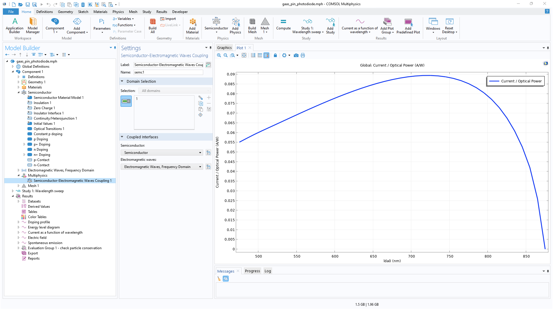
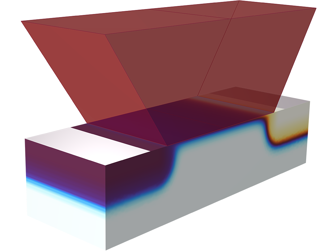
The Semiconductor Module includes two multiphysics interfaces for modeling the interaction of electromagnetic waves and semiconductors. To use this functionality, the Wave Optics Module is required. The functionality is based on the Frequency Domain interfaces and Beam Envelopes interface within the Wave Optics Module.
Couplings between Semiconductor and Electromagnetic Waves interfaces take place through the Optical Transitions feature in the Semiconductor Module. This feature introduces a stimulated emission generation term on domains within the Semiconductor interface, which is appropriate for direct-band-gap materials. This term is proportional to the optical intensity in the corresponding feature in the Electromagnetic Waves interface. Furthermore, the Optical Transitions feature can also account for spontaneous emission in direct-band-gap materials.
The effect of the light absorption or emission is accounted for by a corresponding change in the complex permittivity or refractive index.
Coupled physical effects often play important roles in semiconductor device performance. By combining different physics, such as electrostatics, heat transfer, wave optics, ray optics, and chemical species transport, multiphysics simulations can capture the complex interactions that occur within semiconductor devices. Examples of multiphysics analysis of semiconductor devices include:
Combining the Semiconductor Module with other products in the COMSOL product suite enables multiphysics analysis that provides a more realistic and comprehensive understanding of semiconductor device behavior. This can lead to the development of more efficient and advanced semiconductor devices, with improved performance and capabilities.
Every business and every simulation need is different.
In order to fully evaluate whether or not the COMSOL Multiphysics® software will meet your requirements, you need to contact us. By talking to one of our sales representatives, you will get personalized recommendations and fully documented examples to help you get the most out of your evaluation and guide you to choose the best license option to suit your needs.
Just click on the "Contact COMSOL" button, fill in your contact details and any specific comments or questions, and submit. You will receive a response from a sales representative within one business day.
Request a Software Demonstration